-
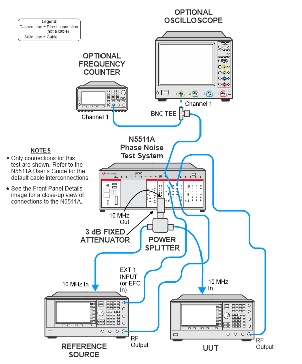
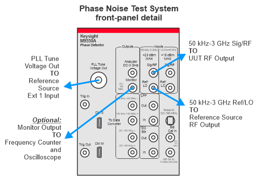
Connect all test equipment as shown.
-
For the 10 MHz connections:
- Connect the 10 MHz Out of the M9300A Frequency Reference Module to the 3 dB attenuator and then to the power splitter.
-
Connect the outputs of the power splitter to the 10 MHz frequency reference of both the DUT and the Reference Source.
-
Connect GPIB cables to all GPIB-controlled test equipment.
-
Preset all test equipment and the DUT.
-
Change the following parameters in the N5510A PNTS user interface:
-
Select the View pull-down menu.
-
Select Display Preferences and un-check the Spurs box.
-
Select OK to close Display Preferences.
-
Select the System pull-down menu and select Server Hardware Connections.
-
Select or ensure the following:
- Test Set has Keysight M9550A selected.
-
FFT Analyzer has Keysight M9551A selected.
-
Select Close to close Server Hardware Connections.
-
Select the Define pull-down menu, select Measurement, and select the following settings:
|
Parameter |
Setting |
|
|
|
|
Type and Range Tab |
|
|
Measurement Type |
Absolute phase noise (using a phase locked loop) |
|
Measurement Method |
Fast |
|
Start Offset Resolution Expansion |
10 |
|
Channel Setup |
Single |
|
Start Offset Frequency |
9 Hz (must be < first specified offset frequency) |
|
Stop Offset Frequency |
110 kHz (must be > last specified offset frequency) |
|
FFT Analyzer Minimum Number of Trace Averages |
160 |
|
RBW % |
1.96 (1024 point FFT) |
|
FFT Overlap % |
75 |
|
FFT Window Type |
Flat Top |
|
|
|
|
Sources Tab |
|
|
Carrier Source Frequency |
Obtain tested frequencies from the TME data entry form. |
|
Carrier Source Power |
+10 dBm |
|
Detector Input Frequency |
Same as Carrier Source Frequency |
|
Reference Source Power |
+15 dBm |
|
VCO Nominal Tune Constant |
1 Hz/Volt |
|
VCO Tune Range |
1 Volt |
|
VCO Input Resistance |
50 Ω |
|
Center Voltage |
0 |
|
|
|
|
Cal Tab |
|
|
Phase Detector Constant |
Derive detector constant from measured beat note |
|
VCO Tune Constant |
Measure VCO Tune Constant |
|
Verify calculated phase lock loop suppression |
Blank |
|
|
|
|
Block Diagram Tab |
|
|
Carrier Source |
Manual |
|
Reference Source |
Model number of reference source |
|
Phase Detector |
Automatic Detector Selection |
|
Test Set Tune Voltage Output |
Front Panel |
|
Test Set Tune Voltage Destination |
Reference Source |
|
VCO Tune Mode |
DCFM |
|
|
|
|
Test Set Tab |
|
|
LNA Low Pass Filter |
Internal — Selected Auto — Checked |
|
LNA Gain |
Auto Gain — Selected Minimum Auto Gain — 14 dB |
|
PLL Integrator Attenuation |
0 dB |
|
Use Channel #2 |
Unchecked |
|
|
|
|
Graph Tab |
|
|
Title |
User specified |
|
Graph Type |
Single-sideband phase noise (dBc/Hz) |
|
X Scale minimum |
Same as start offset frequency |
|
X Scale maximum |
Same as stop offset frequency |
|
Y Scale maximum |
0 dBc/Hz |
|
Y Scale minimum |
–170 dBc/Hz |
|
Normalize Trace Data |
1 Hz bandwidth |
|
Trace Smoothing Amount |
0 |

Making the Measurement
-
Set the DUT frequency to the first carrier frequency and power in the TME data entry form.
-
Set the DUT RF Output to On.
-
If testing a DUT with Option UNX, UNY, or HNY, ensure that the Optimize φ Noise is set to Optimize φ Noise Offset < 150 kHz (Mode 1). To do this, press Frequency > More > More > Optimize φ Noise and select Optimize φ Noise Offset < 150 kHz (Mode 1).
-
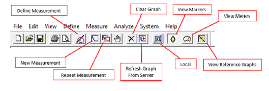
Select the Measure pull-down menu and select New Measurement.
-
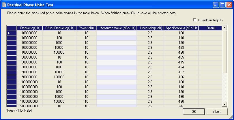
When the measurement completes, select the Markers icon and place markers at specified offsets to determine the measured phase noise. When specifying a marker offset, the marker will be set to the closest frequency on the graph as indicated in the following table:
Nominal Offset
Actual Offset
10 Hz
10.058 Hz
100 Hz
99.838 Hz
1 kHz
1.0014 kHz
10 kHz
9.9182 kHz
20 kHz
19.836 kHz
100 kHz
100.71 kHz