This test uses a phase noise test system to verify that the PSG-D signal generator meets the single-sideband phase noise specifications. The reference source used should have equal or better phase noise specifications compared to the DUT. If the DUT fails, it may be due to the phase noise contributions of the reference source. If a failure occurs, a three-source comparison should be done at the failed carrier frequency and offset to identify a true failure.
|
Test Equipment |
Recommended Models |
Alternate Model(s) |
|
Phase Noise System |
N5511A Options 540, CH21
|
E5505A Option 001
|
|
Reference Source |
E8257D Opt UNT, UNY, and 1EU E8257D/E8663D Opt HY21
|
E8257D Opt UNT, UNR1 or UNX1 or HNY3, and 1EU E8663D Opt UNT, UNX1 or UNY and 1EU E8247C Opt UNR1 8662A2
|
|
6 dB Attenuator |
8490D Opt 006 |
8493C Opt 006 |
Consult the TME data entry form for this test to determine the test conditions for:
Measurement modes (see next section)
There are three measurement modes for this test:
SNR Mode — Option HY2 only
Corresponds to the following states in the data entry form:
SNR Mode = false (or the column is not present)
Tested with the DUT power set to +10 dBm or maximum output power, whichever is less. Consult the TME data entry form for the exact value.
Corresponds to the following states in the data entry form:
SNR Mode = false (or the column is not present)
Tested with the DUT power set to +16 dBm or maximum achievable power, whichever is less.
Corresponds to the following states in the data entry form:
SNR mode = true
Carrier (DUT) power:
For other carrier frequencies: +10 dBm or maximum output power, whichever is less. Consult the TME data entry form for the exact value.
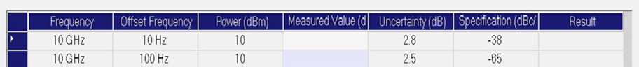
The values required for this test can be found on the TME data entry form. The form is generated in TME when the Single-Sideband Phase Noise test is started.
The table below explains the terms used in the test and their corresponding ![]() columns in the data entry form.
columns in the data entry form.
|
Test Value |
TME Data Entry Form Column Header |
|
Carrier (DUT) frequency |
Frequency |
|
Carrier (DUT) power |
Power (dBm) |
|
Measured offset frequencies |
Offset Frequency |
|
|
|
There are two sets of procedures depending on the model of the phase noise test system used:
E5505A, E5504A/B, and E5503A/B, legacy phase noise test systems
Select from the links below according to the phase noise test system being used.
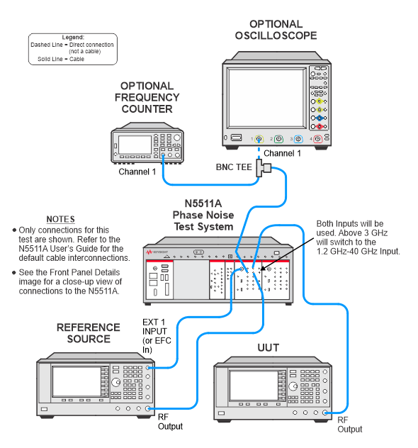
Connect all test equipment as shown.
Connect GPIB cables to all GPIB-controlled test equipment.
Preset all test equipment and the DUT.
Change the following parameters in the N5510A PNTS user interface:
Select the View pull-down menu.
Select Display Preferences and un-check the Spurs box.
Select OK to close Display Preferences.
Select the System pull-down menu and select Server Hardware Connections.
Select or ensure the following:
FFT Analyzer has Keysight M9551A selected.
Select Close to close Server Hardware Connections.
Select the Define
pull-down menu, select Measurement, and select the
following settings:
|
Parameter |
Setting |
||||||||||||||
|
|
|
||||||||||||||
|
Type and Range Tab |
|||||||||||||||
|
Measurement Type |
Absolute phase noise (using a phase locked loop) |
||||||||||||||
|
Measurement Method |
Fast |
||||||||||||||
|
Start Offset Resolution Expansion |
10 |
||||||||||||||
|
Channel Setup |
Single |
||||||||||||||
|
Start Offset Frequency |
0.9 Hz (must be < first specified offset frequency) |
||||||||||||||
|
Stop Offset Frequency |
110 MHz (must be > last specified offset frequency) Limited to:
|
||||||||||||||
|
FFT Analyzer Minimum Number of Trace Averages |
40 |
||||||||||||||
|
RBW % |
7.84 (256 point FFT) |
||||||||||||||
|
FFT Overlap % |
75 |
||||||||||||||
|
FFT Window Type |
Flat Top |
||||||||||||||
|
|
|
||||||||||||||
|
Sources Tab |
|||||||||||||||
|
Carrier Source Frequency |
Obtain tested frequencies from the TME data entry form. |
||||||||||||||
|
Carrier Source Power |
The carrier source power should be set to the power for which the phase noise specification applies. Phase noise is specified at +10 dBm or maximum specified output power, whichever is less. Low Phase Noise ModeThe low phase noise mode is specified at +16 dBm (+13 dBm for E8663D Option HY2) or maximum achievable power, whichever is less. If the power is unleveled at +16 dBm (+13 dBm for E8663D Option HY2), the power is decremented in steps of 0.1 dB until it is leveled, then tested at this power. |
||||||||||||||
|
Detector Input Frequency |
Same as Carrier Source Frequency |
||||||||||||||
|
Reference Source Power |
+15 dBm to 3 GHz |
||||||||||||||
|
VCO Nominal Tune Constant |
|
||||||||||||||
|
VCO Tune Range |
|
||||||||||||||
|
VCO Input Resistance |
|
||||||||||||||
|
Center Voltage |
0 |
||||||||||||||
|
|
|
||||||||||||||
|
Cal Tab |
|||||||||||||||
|
Phase Detector Constant |
Derive detector constant from measured beat note |
||||||||||||||
|
VCO Tune Constant |
Measure VCO Tune Constant |
||||||||||||||
|
Verify calculated phase lock loop suppression |
Blank |
||||||||||||||
|
|
|
||||||||||||||
|
Block Diagram Tab |
|||||||||||||||
|
Carrier Source |
Manual |
||||||||||||||
|
Reference Source |
Model number of reference source |
||||||||||||||
|
Phase Detector |
Automatic Detector Selection |
||||||||||||||
|
Test Set Tune Voltage Output |
Front Panel |
||||||||||||||
|
Test Set Tune Voltage Destination |
Reference Source |
||||||||||||||
|
VCO Tune Mode |
|
||||||||||||||
|
|
|
||||||||||||||
|
Test Set Tab |
|||||||||||||||
|
LNA Low Pass Filter |
Internal — Selected Auto — Checked |
||||||||||||||
|
LNA Gain |
Auto Gain — Selected Minimum Auto Gain — 14 dB |
||||||||||||||
|
PLL Integrator Attenuation |
0 dB |
||||||||||||||
|
Use Channel #2 |
Unchecked |
||||||||||||||
|
|
|
||||||||||||||
|
Graph Tab |
|||||||||||||||
|
Title |
User specified |
||||||||||||||
|
Graph Type |
Single-sideband phase noise (dBc/Hz) |
||||||||||||||
|
X Scale minimum |
Same as start offset frequency |
||||||||||||||
|
X Scale maximum |
Same as stop offset frequency |
||||||||||||||
|
Y Scale maximum |
0 dBc/Hz |
||||||||||||||
|
Y Scale minimum |
–170 dBc/Hz |
||||||||||||||
|
Normalize Trace Data |
1 Hz bandwidth |
||||||||||||||
|
Trace Smoothing Amount |
0 |
||||||||||||||

Making the Measurement
Set the DUT frequency to the first carrier frequency and power in the TME data entry form.
Set the DUT RF Output to On.
Ensure that the 10 MHz reference of the DUT is set to internal. (The EXT REF annunciator should not be displayed. If it is, check for a signal going to the 10 MHz IN connector.)
If testing a DUT with Option UNX, UNY, or HNY, ensure that the Optimize φ Noise is set to Optimize φ Noise Offset < 150 kHz (Mode 1). To do this, press Frequency > More > More > Optimize φ Noise and select Optimize φ Noise Offset < 150 kHz (Mode 1).
If testing a DUT in Standard mode:
If the DUT has Option HY2, set the DUT's Optimize Signal Noise mode to OFF. (Presetting the DUT turns Optimize Signal Noise mode to ON.) To do this, perform the following steps in order:
Press Amplitude > More > More > Optimize S/N Off On and select Off.
Press Frequency > More > RF Path and select Normal.
Press Frequency > More > Low Pass Filter Below 2 GHz and select Off.
If testing a DUT in Low Phase Noise mode:
If testing Option UNX, UNY, or HNY, turn on Low Phase Noise Below 250 MHz. Select Frequency > More > More > RF Path and select Low Phase Noise Below 250 MHz.
If testing Option HAR, turn on Optimize Noise Below 500 MHz. Select Frequency > More > More > Optimize noise below 500 MHz and select On.
If testing a DUT in SNR mode, set the DUT's Optimize Signal Noise mode to ON. To do this, perform the following steps in order:
Press Amplitude > More > More > Optimize S/N Off On and select On.
Press Frequency > More > RF Path and select Low Phase Noise Below 250 MHz.
Press Frequency > More > Low Pass Filter Below 2 GHz and select Off.
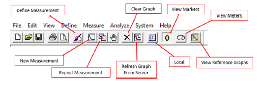
Select the Measure pull-down menu and select New Measurement.
When the measurement completes, select the Markers icon and place markers at specified offsets to determine the measured phase noise. When specifying a marker offset, the marker will be set to the closest frequency on the graph as indicated in the following table:
|
Nominal Offset |
Actual Offset |
|
1 Hz |
1.0245 Hz |
|
10 Hz |
10.058 Hz |
|
100 Hz |
99.838 Hz |
|
1 kHz |
1.0014 kHz |
|
10 kHz |
9.9182 kHz |
|
20 kHz |
19.836 kHz |
|
100 kHz |
100.71 kHz |
|
1 MHz |
1.001 MHz |
|
10 MHz |
10.059 MHz |
|
100 MHz |
100 MHz |
For carrier frequencies above 3 GHz, the following connection changes are required:
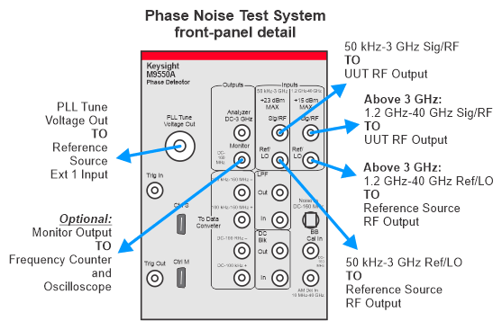
Connect the Reference Source Output to the 1.2 GHz to 40 GHz Ref/LO Input of the M9550A Phase Detector module in the N5511A PNTS.
If a failure occurs, a three-source comparison measurement should be performed at the same carrier frequency to identify a true failure.
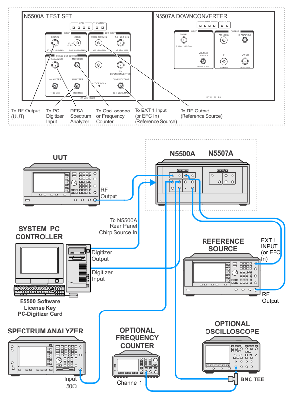
Connect all test equipment as shown.
Connect GPIB cables to all GPIB-controlled test equipment.
Preset all test equipment and the DUT.
When measuring Standard Mode, in the E5505A Phase Noise System user interface, change the following parameters:
Select the View pull-down menu.
Select Display Preferences and un-check the Spurs box.
Select OK to close Display Preferences.
Select the System pull-down menu and select Server Hardware Connections.
Select or ensure that the FFT Analyzer has NI PCI6111-1, 11 PCI20428W-1, or 89410A selected.
Select Close to close Server Hardware Connections.
Select the Define
pull-down menu, select Measurement, and select the
following settings:
|
Parameter |
Setting |
|||||||||||||||||||||||||||||||||||
|
|
|
|||||||||||||||||||||||||||||||||||
|
Type and Range Tab |
||||||||||||||||||||||||||||||||||||
|
Measurement Type |
Absolute phase noise (using a phase locked loop) |
|||||||||||||||||||||||||||||||||||
|
Start Offset Frequency |
1 Hz (must be ≤ first specified offset frequency) |
|||||||||||||||||||||||||||||||||||
|
Stop Offset Frequency |
100 MHz (must be ≥ last specified offset frequency) Note: Can be no more than the carrier frequency/5. For example, for a carrier frequency of 10 MHz, this is limited to 2 MHz. |
|||||||||||||||||||||||||||||||||||
|
FFT Analyzer Minimum Number of Averages |
1 |
|||||||||||||||||||||||||||||||||||
|
FFT Quality |
Custom |
|||||||||||||||||||||||||||||||||||
|
Define Custom Segment Table — FFT Note: the following parameters should be left at their default values for all segments:
|
|
|||||||||||||||||||||||||||||||||||
|
Swept Quality |
Custom |
|||||||||||||||||||||||||||||||||||
|
Define Custom Segment Table — Swept Note: the following parameters should be left at their default values for all segments:
|
|
|||||||||||||||||||||||||||||||||||
|
|
|
|||||||||||||||||||||||||||||||||||
|
Sources Tab |
||||||||||||||||||||||||||||||||||||
|
Carrier Source Connected |
Test Set |
|||||||||||||||||||||||||||||||||||
|
Carrier Source Frequency |
Obtain tested frequencies from the TME data entry form. |
|||||||||||||||||||||||||||||||||||
|
Carrier Source Power |
Obtain from the TME data entry form. When testing at +16 dBm or maximum achievable output power, first set the DUT power to +16 dBm (+13 dBm for E8663D Option HY2). If the power is unleveled at +16 dBm (+13 dBm for E8663D Option HY2), decrement the power in steps of 0.1 dB until it is leveled; test at this power. |
|||||||||||||||||||||||||||||||||||
|
Detector Input Frequency |
Same as Carrier Source Frequency |
|||||||||||||||||||||||||||||||||||
|
Reference Source Power |
+15 dBm for Carrier Source Frequency ≤ 1.6 GHz |
|||||||||||||||||||||||||||||||||||
|
VCO Tune Constant |
|
|||||||||||||||||||||||||||||||||||
|
VCO Tune Range |
|
|||||||||||||||||||||||||||||||||||
|
VCO Input Resistance |
|
|||||||||||||||||||||||||||||||||||
|
Center Voltage |
0 |
|||||||||||||||||||||||||||||||||||
|
|
|
|||||||||||||||||||||||||||||||||||
|
Cal Tab |
||||||||||||||||||||||||||||||||||||
|
Phase Detector Constant |
Measure Phase Detector Constant |
|||||||||||||||||||||||||||||||||||
|
VCO Tune Constant |
Measure VCO Tune Constant |
|||||||||||||||||||||||||||||||||||
|
Verify calculated phase lock loop suppression |
Blank |
|||||||||||||||||||||||||||||||||||
|
|
|
|||||||||||||||||||||||||||||||||||
|
Block Diagram Tab |
||||||||||||||||||||||||||||||||||||
|
Carrier Source |
Manual |
|||||||||||||||||||||||||||||||||||
|
Down Converter |
None |
|||||||||||||||||||||||||||||||||||
|
Reference Source |
Model number of reference source |
|||||||||||||||||||||||||||||||||||
|
Phase Detector |
Automatic Detector Selection |
|||||||||||||||||||||||||||||||||||
|
Test Set Tune Voltage Output |
Front Panel |
|||||||||||||||||||||||||||||||||||
|
Test Set Tune Voltage Destination |
Reference Source |
|||||||||||||||||||||||||||||||||||
|
VCO Tune Mode |
|
|||||||||||||||||||||||||||||||||||
|
|
|
|||||||||||||||||||||||||||||||||||
|
Test Set Tab |
||||||||||||||||||||||||||||||||||||
|
Input Attenuation |
0 dB |
|||||||||||||||||||||||||||||||||||
|
LNA Low Pass Filter |
Auto |
|||||||||||||||||||||||||||||||||||
|
LNA Gain |
Auto Gain |
|||||||||||||||||||||||||||||||||||
|
Minimum Auto Gain |
14 dB |
|||||||||||||||||||||||||||||||||||
|
PLL Integrator Attenuation |
0 dB |
|||||||||||||||||||||||||||||||||||
|
|
|
|||||||||||||||||||||||||||||||||||
|
Graph Tab |
||||||||||||||||||||||||||||||||||||
|
Title |
User specific |
|||||||||||||||||||||||||||||||||||
|
Graph Type |
Single-sideband phase noise (dBc/Hz) |
|||||||||||||||||||||||||||||||||||
|
X Scale minimum |
Same as start offset frequency |
|||||||||||||||||||||||||||||||||||
|
X Scale maximum |
Same as stop offset frequency |
|||||||||||||||||||||||||||||||||||
|
Y Scale minimum |
0 dBm |
|||||||||||||||||||||||||||||||||||
|
Y Scale maximum |
–170 dBm |
|||||||||||||||||||||||||||||||||||
|
Normalize Trace Data |
1 Hz bandwidth |
|||||||||||||||||||||||||||||||||||
|
Trace Smoothing Amount |
0 |
|||||||||||||||||||||||||||||||||||
Making the Measurement
Set the DUT frequency to the first carrier frequency and power in the TME data entry form.
Set the DUT RF Output to On.
Ensure that the 10 MHz reference of the DUT is set to internal. (The EXT REF annunciator should not be displayed. If it is, check for a signal going to the 10 MHz IN connector.)
If testing a DUT with Option UNX, UNY, or HNY, ensure that the Optimize φ Noise is set to Optimize φ Noise Offset < 150 kHz (Mode 1). To do this, press Frequency > More > MoreOptimize φ Noise and select Optimize φ Noise Offset < 150 kHz (Mode 1).
If testing a DUT in Standard mode:
If the DUT has Option HY2, set the DUT's Optimize Signal Noise mode to OFF. (Presetting the DUT turns Optimize Signal Noise mode to ON.) To do this, perform the following steps in order:
Press Amplitude > More > More > Optimize S/N Off On and select Off.
Press Frequency > More > RF Path and select Normal.
Press Frequency > More > Low Pass Filter Below 2 GHz and select Off.
If testing a DUT in Low Phase Noise mode:
If testing Option UNX, UNY, or HNY, turn on Low Phase Noise Below 250 MHz. Select Frequency > More > More > RF Path and select Low Phase Noise Below 250 MHz.
If testing Option HAR, turn on Optimize Noise Below 500 MHz. Select Frequency > More > More > Optimize noise below 500 MHz and select On.
If testing a DUT in SNR mode, set the DUT's Optimize Signal Noise mode to ON. To do this, perform the following steps in order:
Press Amplitude > More > More > Optimize S/N Off On and select On.
Press Frequency > More > RF Path and select Low Phase Noise Below 250 MHz.
Press Frequency > More > Low Pass Filter Below 2 GHz and select Off.
Select the Measure pull-down menu and select New Measurement.
When the measurement completes, select the Markers icon and place markers at the offsets specified in the TME data entry form. To get these offsets, follow the steps below:
Launch TME with the DUT connected to the test system.
Start the Single-Sideband Phase Noise test.
With the form selected, press Ctrl-A, Ctrl-C on the keyboard to collect the data in the form.
Open an application such as Microsoft Notepad and press Ctrl-V to copy the test point data into this application.
Print out this data and use it to complete this test.
Continue to the next carrier frequency and/or measurement mode and perform the measurement. Note the following frequency specific changes:
Above 1.6 GHz:
Move the reference source RF Output to the 1.2-26.5 GHz REF INPUT from the 50 kHz-1600 MHz REF INPUT.
The Reference Source Power is reduced from +15 dBm to +10 dBm.
If the Phase Noise test set is not equipped with Option 001 (which permits up to +30 dBm input power), then the signal from the DUT to the test set must be limited to +5 dBm. Insert a 6 dB attenuator between the DUT RF Output and the Phase Noise test set signal input if the Carrier (DUT) Source Power is set above +5 dBm.
If a failure occurs, a three-source comparison measurement should be performed at the same carrier frequency to identify a true failure.
|
|
|
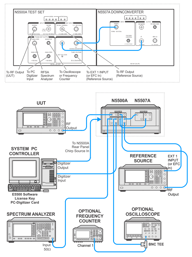
The equipment is connected as shown below. These connections are identical to the Standard Method except for the two additional connections between the downconverter and the test set.
The procedure is identical to that for the Standard Method except for the following:
Measurement settings
|
Parameter |
Setting |
|
Sources Tab: |
|
|
Carrier Source Connected |
Downconverter |
|
Reference Source Power |
+15 dBm (all frequencies) |
|
Block Diagram Tab: |
|
|
Down Converter |
System Control |
|
Downconverter Tab: |
|
|
Input Attenuation |
Auto |
|
IF Gain |
Auto |
|
Microwave/Millimeter Band |
Microwave (0–26.5 GHz) |
|
Reference Chain Reference |
10 MHz |
|
External Tune Enable |
Blank |
During the measurement, the reference source remains connected to the 50 kHz–1600 MHz Ref Input and is never connected to the 1.2–26.5 GHz Ref Input.
Unlike the Standard Method, the three-source comparison measurement procedure does not produce valid results when using the downconverter method and therefore may not be used.
If this performance test fails, perform the following steps in order:
Check the equipment setup (see above). If the setup is incorrect, make the necessary corrections and rerun the Performance Test.
If this test fails with the equipment setup properly, refer to the troubleshooting section of the signal generator's service guide.If you do not have a printed copy of the service guide (Option OBW), one is available either on the CD-ROM that came with your signal generator shipment or on the Keysight Website.
If you cannot correct the problem using the troubleshooting procedures in the Service Guide, obtain service from Keysight Technologies. Refer to Contacting Keysight Technologies.
