Single Sideband Phase Noise — E4438C Option UNJ and E4428C Only
(Manual Performance Test)
This manual test verifies that the signal generator's single sideband
phase noise meets specification. During this test, a phase noise system
and a reference source are used to measure the single sideband phase noise
of the signal generator. The phase noise is measured at 20 kHz offsets
to different test frequencies and compared to specifications.
If a failure occurs, it may not be due to the signal generator. For
some test conditions, the signal generator specifications are better than
the reference source specifications. If a failure occurs, a three-source comparison should be performed at this carrier frequency to identify
a true failure.
|

|
When mapping the Phase Noise Reference Source in TME,
the sources you can choose from are prefixed with "PNRS_"
(e.g., "PNRS_E8257D"). This prefix is used to distinguish
these sources from the sources that must be on the GPIB
bus (the Reference Source is not required to be on the bus). If you map
the same device as a Reference Source and as something else, you will
need to enter the serial number and calibration due date each time because
TME treats each mapping as a different device.
|
|
Test Equipment
|
Recommended Models
|
Alternate Models
|
|
Phase Noise System
|
N5511A Options 540, CH21
|
E5505A
E5501A/B
E5502A/B
E5503A/B
E5504A/B
|
|
Reference Source2
|
E8257D3 Opt UNR, UNX, or UNY
|
8664A Opt 004,
8665A Opt 004,
8665B Opt 004,
E8247C Opt UNR,
E8257C Opt UNR,
E8267C Opt UNR,
E8267D Opt UNR, UNX, or UNY
E8663B
E8663D Opt UNX or UNY
|
|
Cable
|
8120-4921 APC 3.5 (m) to (m)
|
|
|
Cable
|
11500C
Type-N (m) to (m)
|
|
|
Cable
|
8120-1840 BNC (m) to (m)
10503A BNC (m) to (m)
|
|
|
Adapter
|
E9625A BNC Tee (m) (f) (f)
|
|
|
Adapter
|
11901D 2.4 mm (f) to APC 3.5
(m)
|
|
|
Adapter
|
1250-1749
APC 3.5 (f) to (f)
|
|
- CH2 is not required but recommended for future capability.
- The reference source must have a frequency high enough based on the test points being tested. Note that test points are not the same as the frequency range of the DUT. Therefore, some alternative models may not be sufficient for all DUTs. The E8257D recommended model is sufficient for all DUT configurations.
- Option 1EA or 1EU is not required providing that the LO in use has leveled output
power at each test frequency.
|
Connections and Setup Procedures for a 500 MHz Single-Sideband Phase Noise Measurement
|
|
- All test equipment requires
a 30 minute warmup period to ensure accurate performance.
- In the following test setup,
cables are designated as solid lines and direct connections are designated
as dashed lines.
|
There are two sets of procedures depending on the model of the phase noise test system used:
-
N5511A Phase Noise Test System (PNTS), recommended phase noise test system
-
E550xA/B, legacy phase noise test systems
Select from the links below according to the phase noise test system being used.
N5511A PNTS, standard method  click here.
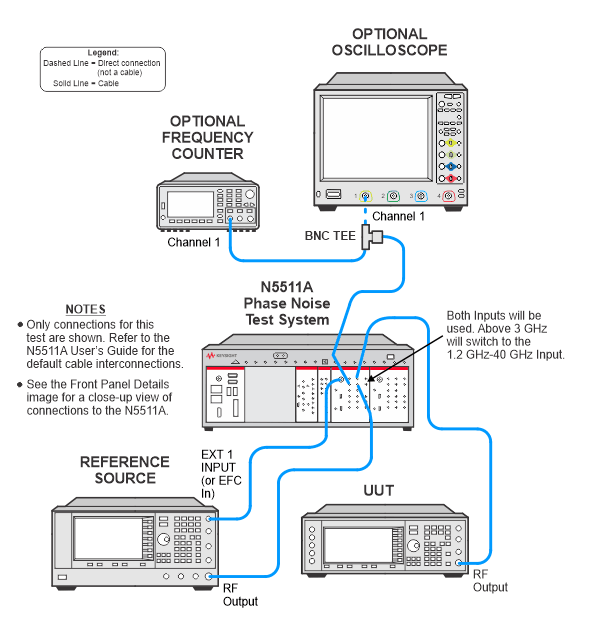
-
Connect
all test equipment as shown.
-
Connect
GPIB cables to all GPIB-controlled test equipment.
-
Preset
all test equipment and the DUT.
-
Change the following parameters in
the :
-
Select the View
pull-down menu.
-
Select Display
Preferences and un-check the Spurs box.
-
Select OK
to close Display Preferences.
-
Select the System pull-down menu and select Server Hardware Connections.
-
Select or ensure the following:
- Test Set has Keysight M9550A selected.
-
FFT Analyzer has Keysight M9551A selected.
-
Select Close to close Server Hardware Connections.
-
Select the Define
pull-down menu, select Measurement, and select the
following settings:
|
Parameter
|
Setting
|
|
|
|
|
Type and Range Tab
|
|
Measurement Type
|
Absolute phase noise (using a phase locked loop)
|
|
Measurement Method
|
Fast
|
|
Start Offset Resolution Expansion
|
10
|
|
Channel Setup
|
Single
|
|
Start Offset Frequency
|
0.9 Hz (must be < first specified offset frequency)
|
|
Stop Offset Frequency
|
110 MHz (must be > last specified offset frequency)
Limited to:
- 200 kHz offset at 1 MHz
- 2 MHz offset at 10 MHz
- 20 MHz offset at 100 MHz
- 100 MHz offset at ≥250 MHz
|
|
FFT Analyzer Minimum Number of Trace Averages
|
40
|
|
RBW %
|
7.84 (256 point FFT)
|
|
FFT Overlap %
|
75
|
|
FFT Window Type
|
Flat Top
|
|
|
|
|
Sources Tab
|
|
Carrier Source Frequency
|
Obtain tested frequencies from the TME data entry form.
|
|
Carrier Source Power
|
The carrier source power should be set to the power for which the phase noise specification applies.
The ESG-C does not specify a power level. Historically it has been tested at +14 dBm up to 1 GHz, and +10 dBm at ≥ 2 GHz.
|
|
Detector Input Frequency
|
Same as Carrier Source Frequency
|
|
Reference Source Power
|
+15 dBm to 3 GHz
+10 dBm for > 3 GHz
|
|
VCO Nominal Tune Constant
|
|
Based on the reference source:
|
|
|
866xA
|
5e-9 x carrier source frequency
|
Example: 1.25 Hz/Volt at a carrier frequency of 250 MHz
|
|
PSG
|
0.1 ppm x carrier source frequency
|
Example: 25 Hz/Volt at a carrier frequency of 250 MHz
|
|
PSG-D
|
0.12 Hz/V
|
when measuring Low Phase Noise @ 1 MHz
|
|
0.1 ppm x carrier source frequency
|
all other measurements
|
|
|
VCO Tune Range
|
|
Based on the reference source:
|
|
|
866xA
|
10 Volts
|
|
|
PSG
|
5 Volts
|
|
|
PSG-D
|
5 Volts
|
when measuring Low Phase Noise @ 1 MHz
|
|
1 Volt
|
all other measurements
|
|
|
VCO Input Resistance
|
|
Based on the reference source:
|
|
|
866xA
|
1 Mohm
|
|
|
PSG
|
50 ohms
|
|
|
PSG-D
|
1 Mohm
|
when measuring Low Phase Noise @ 1 MHz
|
|
50 ohms
|
all other measurements
|
|
|
Center Voltage
|
0
|
|
|
|
|
Cal Tab
|
|
Phase Detector Constant
|
Derive detector constant from measured beat note
|
|
VCO Tune Constant
|
Measure VCO Tune Constant
|
|
Verify calculated phase lock loop suppression
|
Blank
|
|
|
|
|
Spurious Tab
|
|
Mark Spur
|
Checked
|
|
Minimum Limit
|
4 dB
|
|
Maximum Limit
|
50 dB
|
|
|
|
|
Block Diagram Tab
|
|
Carrier Source
|
Manual
|
|
Reference Source
|
Model number of reference source
|
|
Phase Detector
|
Automatic Detector Selection
|
|
Test Set Tune Voltage Output
|
Front Panel
|
|
Test Set Tune Voltage Destination
|
Reference Source
|
|
VCO Tune Mode
|
|
Based on the reference source:
|
|
|
866xA
|
EFC
|
|
|
PSG
|
DCFM
|
|
|
PSG-D
|
EFC
|
when measuring Low Phase Noise @ 1 MHz
|
|
DCFM
|
all other measurements
|
|
|
|
|
|
Test Set Tab
|
|
LNA Low Pass Filter
|
Internal — Selected
Auto — Checked
|
|
LNA Gain
|
Auto Gain — Selected
Minimum Auto Gain — 14 dB
|
|
PLL Integrator Attenuation
|
0 dB
|
|
Use Channel #2
|
Unchecked
|
|
|
|
|
Graph Tab
|
|
Title
|
User specified
|
|
Graph Type
|
Single-sideband phase noise (dBc/Hz)
|
|
X Scale minimum
|
Same as start offset frequency
|
|
X Scale maximum
|
Same as stop offset frequency
|
|
Y Scale maximum
|
0 dBc/Hz
|
|
Y Scale minimum
|
–170 dBc/Hz
|
|
Normalize Trace Data
|
1 Hz bandwidth
|
|
Trace Smoothing Amount
|
0
|

Making
the Measurement
-
Set
the DUT frequency to the first carrier frequency and power in the TME data entry form.
-
Set
the DUT RF Output to On.
-
Ensure that the 10 MHz reference of the DUT is set to internal. (The EXT REF annunciator should not be displayed. If it is, check for a signal going to the 10 MHz IN connector.)
-
If testing a DUT with Option UNX, UNY, or HNY, ensure that the Optimize φ Noise is set to Optimize φ Noise Offset < 150 kHz (Mode 1). To do this, press Frequency > More > MoreOptimize φ
Noise and select Optimize φ Noise Offset < 150 kHz (Mode 1).
-
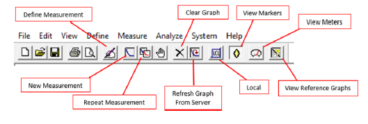
Select
the Measure pull-down menu and select New
Measurement.
-
When the measurement completes,
select the Markers icon and place
markers at specified offsets to determine the measured phase noise. When specifying a marker offset, the marker will be set to the closest frequency on the graph as indicated in the following table:
|
Nominal Offset
|
Actual Offset
|
|
1 Hz
|
1.0245 Hz
|
|
10 Hz
|
10.058 Hz
|
|
100 Hz
|
99.838 Hz
|
|
1 kHz
|
1.0014 kHz
|
|
10 kHz
|
9.9182 kHz
|
|
20 kHz
|
19.836 kHz
|
|
100 kHz
|
100.71 kHz
|
|
1 MHz
|
1.001 MHz
|
|
10 MHz
|
10.059 MHz
|
|
100 MHz
|
100 MHz
|
-
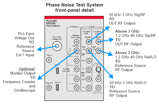
For carrier frequencies above 3 GHz, the following connection changes are required:
- Connect the UUT RF Output to the 1.2 GHz to 40 GHz Sig/RF Input of the M9550A Phase Detector module in the N5511A PNTS.
-
Connect the Reference Source Output to the 1.2 GHz to 40 GHz Ref/LO Input of the M9550A Phase Detector module in the N5511A PNTS.
-
If a failure occurs, a three-source comparison measurement should be performed at the same carrier frequency to identify a true failure.
E550xA/B legacy phase noise test systems, click here.
- Connect
all test equipment as shown.
- Connect
GPIB cables to all GPIB-controlled test equipment.
- While
performing this adjustment, follow all instructions on the
controller display.
Setup with
a carrier frequency of 500 MHz
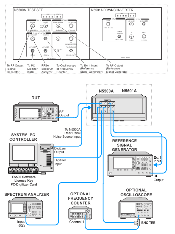
-
Connect all test equipment as shown.
-
Connect GPIB cables to all GPIB-controlled test equipment.
-
Preset all test equipment and the signal generator.
-
Connect the E8257D RF output to the N5500A reference
input.
-
Connect the N5500A Tune Voltage Output to the E8257D
Ext 1 input.
|
Table 1: E4438C and E4428C Carrier Test Frequencies and
Power
|
|
Frequency (MHz)
|
DUT Power (dBm)
|
Reference Power (dBm)
|
|
500
|
14
|
12
|
|
1000
|
14
|
12
|
|
2000
|
10
|
5
|
|
3000
|
10
|
5
|
|
4000
|
10
|
5
|
|
6000
|
10
|
5
|
-
In the Keysight N5505A Phase Noise System user interface,
change the following parameters:
-
Select the
View pull down menu.
-
Select Display Preferences and clear the Spurs box.
-
Select OK to close Display Preferences.
-
From the System pull down menu, select Server Hardware Connections.
-
Ensure the
correct FFT Analyzer is selected, either the 11 PCI20428W-1 or the 89410A.
-
Connect
the signal generator's RF OUTPUT to the N5500A signal input.
-
Connect
the 70420A or N5500A 50 kHz to 1600 MHz Reference Input to the Reference
Generator RF Out.
-
Connect
the 70420A or N5500A Tune Voltage Output to either the FM input (8665B)
or the Ext 1 (PSG) input of the Reference Source.
-
From the Define pull down menu, select Measurement, and set the following:
|
Parameter
|
Setting
|
|
|
|
|
Type and Range Tab
|
|
Measurement Type
|
Absolute phase noise
|
|
Start Offset Frequency
|
1 Hz
|
|
Stop Offset Frequency
|
1 MHz
|
|
FFT Averages
|
4
|
|
FFT Quality
|
Normal
|
|
Swept Quality
|
Normal
|
|
|
|
|
Sources Tab
|
|
Carrier Source Connected
|
Test Set
|
|
Carrier Source Frequency
|
See Table 1.
|
|
Carrier Source Power
|
See Table 1.
|
|
Detector Input Frequency
|
See Table 1.
|
|
Reference Source Power
|
See Table 1.
|
|
VCO Tune Constant
|
1,000 Hz/Volt
|
|
VCO Tune Range
|
5 volts for PSG
|
|
VCO Input Resistance
|
50 ohms for PSG
|
|
|
|
|
Cal Tab
|
|
Measure Phase Detector Constant
|
Checkmark
|
|
Measure VCO Tune Constant
|
Checkmark
|
|
Verify calculated phase lock loop suppression
|
Blank
|
|
Phase Lock Loop Suppression
|
Use theoretical value.
|
|
|
|
|
Block Diagram Tab
|
|
Carrier Source
|
Manual
|
|
Down Converter
|
None
|
|
Reference Source
|
E8257D
|
|
Phase Detector Mode
|
Automatic
|
|
Test Set Tune Voltage Destination
|
Reference Source
|
|
VCO Tune Mode
|
DCFM
|
|
|
|
|
Test Set Tab
|
|
Input Attenuation
|
0 dB
|
|
LNA Low Pass Filter
|
Auto
|
|
LNA Gain
|
Auto
|
|
PLL Integrator Attenuation
|
0 dB
|
|
|
|
|
Downconverter Tab
|
|
Input Attenuation
|
Auto
|
|
IF Gain
|
Auto
|
|
Microwave/Millimeter Band
|
Microwave (0 –
26.5 GHz)
|
|
Reference Chain Reference
|
10 MHz
|
|
External Tune Enable
|
Checkmark
|
|
|
|
|
Graph Tab
|
|
Title
|
User specific
|
|
Graph Type
|
Single-sideband phase noise (dBc/Hz)
|
|
X Scale minimum
|
1 Hz
|
|
X Scale maximum
|
1E+6
|
|
Y Scale maximum
|
0
|
|
Y Scale minimum
|
–170
|
|
Normalize Trace Data
|
1 Hz bandwidth
|
Making the Measurement
-
Set
the signal generator frequency to the first carrier frequency and power
in Table 1.
-
Set
the RF Output to on.
-
Perform
a phase noise measurement.
-
From
the Measure pull down menu, select
New Measurement.
-
Place
a marker at 20 kHz offset.
-
Compare
the marker amplitude value to the specifications displayed by the software.
-
Print
out a phase noise plot.
Entering the Data
The measurement data must be entered into the following form displayed
on-screen when the test is run. The specifications shown below may differ
from those displayed by the software based on the internal hardware of
the particular DUT.
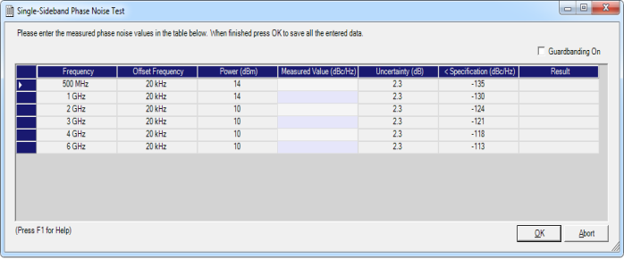
Enter the measured value from the phase noise system into the "Measured
Value" column for the appropriate frequency/offset frequency combination.
All values must be entered for the test to complete. Entering a measured
value and then clicking in the "Result" column in the form will
cause the result to appear.
If the "Guardbanding On" checkbox is not selected, then the
result will be of the form PASS/FAIL. Otherwise, the result will be calculated
using the displayed uncertainty and will be in the form PASS/FAIL/INDETERMINATE.
The specification against which the measured value is compared is displayed
in the "< Specifications" column.
In Case of Difficulty
If this performance test fails, perform the following steps in order:
-
Check the equipment setup (see above). If the setup
is incorrect, make the necessary corrections and rerun the performance
test.
-
If this test fails with the equipment set up properly,
refer to the troubleshooting section of the signal generator's service
guide.
If you do not have a printed copy of the service guide (Option OBW),
one is available either on the CD-ROM that came with your signal generator
shipment or on the Keysight Website.
-
If you cannot correct the problem using the troubleshooting
procedures in the Service Guide,
obtain service from Keysight Technologies. Refer to Contacting Keysight Technologies.