 columns in the data entry form.
This test uses Phase Noise Test System to verify that the signal generator meets the single-sideband phase noise specifications. If the DUT fails, it may be due to the DUT phase noise specifications being better than the reference source. If a failure occurs, a three-source measurement should be done at the failed carrier and offset to identify a true failure.
|
Test Equipment |
Recommended Model |
Alternate Model(s) |
|
Phase Noise Measurement System |
N5511A Options 504, CH21
|
E5505A |
|
Reference Source |
E8257D Option UNT, UNY, and 1EU Output: Type-N (f), APC 3.5 mm (m), 2.4 mm (m) |
E8267D Option UNT, UNY |
|
Cable |
Cable, |
8120-4921 |
|
Cable |
Cable, |
8120-1840
BNC (m) to (m) cable |
The values required for this test can be found on the TME data entry form. The form is generated in TME when the Single-Sideband Phase Noise test is started.
The table below explains the terms used in the test and their corresponding columns in the data entry form.
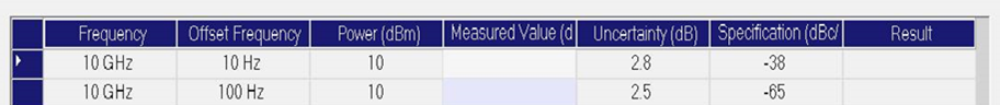
|
Test Value |
TME Data Entry Form Column Header |
|
Carrier (DUT) frequency |
Frequency |
|
Carrier (DUT) power |
Power (dBm) |
|
Measured offset frequencies |
Offset Frequency |
There are two sets of procedures depending on the model of the phase noise test system used:
N5511A Phase Noise Test System (PNTS), recommended phase noise test system
E550xA/B, legacy phase noise test systems
Select from the links below according to the phase noise test system being used.
click here.
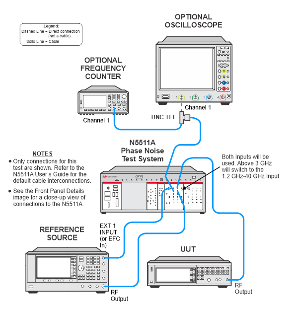
Connect all test equipment as shown.
Connect GPIB cables to all GPIB-controlled test equipment.
Preset all test equipment and the DUT.
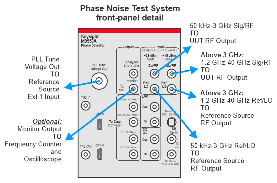
Change the following parameters in the N5510A PNTS user interface:
Select the View pull-down menu.
Select Display Preferences and un-check the Spurs box.
Select OK to close Display Preferences.
Select the System pull-down menu and select Server Hardware Connections.
Select or ensure the following:
FFT Analyzer has Keysight M9551A selected.
Select Close to close Server Hardware Connections.
Select the Define
pull-down menu, select Measurement, and select the
following settings:
|
Parameter |
Setting |
||||||||||||||
|
|
|
||||||||||||||
|
Type and Range Tab |
|||||||||||||||
|
Measurement Type |
Absolute phase noise (using a phase locked loop) |
||||||||||||||
|
Measurement Method |
Fast |
||||||||||||||
|
Start Offset Resolution Expansion |
10 |
||||||||||||||
|
Channel Setup |
Single |
||||||||||||||
|
Start Offset Frequency |
0.9 Hz (must be < first specified offset frequency) |
||||||||||||||
|
Stop Offset Frequency |
110 MHz (must be > last specified offset frequency) Limited to:
|
||||||||||||||
|
FFT Analyzer Minimum Number of Trace Averages |
40 |
||||||||||||||
|
RBW % |
7.84 (256 point FFT) |
||||||||||||||
|
FFT Overlap % |
75 |
||||||||||||||
|
FFT Window Type |
Flat Top |
||||||||||||||
|
|
|
||||||||||||||
|
Sources Tab |
|||||||||||||||
|
Carrier Source Frequency |
Obtain tested frequencies from the TME data entry form. |
||||||||||||||
|
Carrier Source Power |
The carrier source power should be set to the power for which the phase noise specification applies. The N5181B and N5182B are tested at +10 dBm. |
||||||||||||||
|
Detector Input Frequency |
Same as Carrier Source Frequency |
||||||||||||||
|
Reference Source Power |
+15 dBm to 3 GHz |
||||||||||||||
|
VCO Nominal Tune Constant |
|
||||||||||||||
|
VCO Tune Range |
|
||||||||||||||
|
VCO Input Resistance |
|
||||||||||||||
|
Center Voltage |
0 |
||||||||||||||
|
|
|
||||||||||||||
|
Cal Tab |
|||||||||||||||
|
Phase Detector Constant |
Derive detector constant from measured beat note |
||||||||||||||
|
VCO Tune Constant |
Measure VCO Tune Constant |
||||||||||||||
|
Verify calculated phase lock loop suppression |
Blank |
||||||||||||||
|
|
|
||||||||||||||
|
Block Diagram Tab |
|||||||||||||||
|
Carrier Source |
Manual |
||||||||||||||
|
Reference Source |
Model number of reference source |
||||||||||||||
|
Phase Detector |
Automatic Detector Selection |
||||||||||||||
|
Test Set Tune Voltage Output |
Front Panel |
||||||||||||||
|
Test Set Tune Voltage Destination |
Reference Source |
||||||||||||||
|
VCO Tune Mode |
|
||||||||||||||
|
|
|
||||||||||||||
|
Test Set Tab |
|||||||||||||||
|
LNA Low Pass Filter |
Internal — Selected Auto — Checked |
||||||||||||||
|
LNA Gain |
Auto Gain — Selected Minimum Auto Gain — 14 dB |
||||||||||||||
|
PLL Integrator Attenuation |
0 dB |
||||||||||||||
|
Use Channel #2 |
Unchecked |
||||||||||||||
|
|
|
||||||||||||||
|
Graph Tab |
|||||||||||||||
|
Title |
User specified |
||||||||||||||
|
Graph Type |
Single-sideband phase noise (dBc/Hz) |
||||||||||||||
|
X Scale minimum |
Same as start offset frequency |
||||||||||||||
|
X Scale maximum |
Same as stop offset frequency |
||||||||||||||
|
Y Scale maximum |
0 dBc/Hz |
||||||||||||||
|
Y Scale minimum |
–170 dBc/Hz |
||||||||||||||
|
Normalize Trace Data |
1 Hz bandwidth |
||||||||||||||
|
Trace Smoothing Amount |
0 |
||||||||||||||

Making the Measurement
Set the DUT frequency to the first carrier frequency and power in the TME data entry form.
Set the DUT RF Output to On.
Ensure that the 10 MHz reference of the DUT is set to internal. (The EXT REF annunciator should not be displayed. If it is, check for a signal going to the 10 MHz IN connector.)
If testing a DUT with Option UNX or UNY, ensure that the Optimize φ Noise is set to Optimize φ Noise Offset < 150 kHz (Mode 1). To do this, press Frequency > More > More > Optimize φ Noise and select Optimize φ Noise Offset < 150 kHz (Mode 1).
Select the Measure pull-down menu and select New Measurement.
When the measurement completes, select the Markers icon and place markers at specified offsets to determine the measured phase noise. When specifying a marker offset, the marker will be set to the closest frequency on the graph as indicated in the following table:
|
Nominal Offset |
Actual Offset |
|
1 Hz |
1.0245 Hz |
|
10 Hz |
10.058 Hz |
|
100 Hz |
99.838 Hz |
|
1 kHz |
1.0014 kHz |
|
10 kHz |
9.9182 kHz |
|
20 kHz |
19.836 kHz |
|
100 kHz |
100.71 kHz |
|
1 MHz |
1.001 MHz |
|
10 MHz |
10.059 MHz |
|
100 MHz |
100 MHz |
For carrier frequencies above 3 GHz, the following connection changes are required:
Connect the Reference Source Output to the 1.2 GHz to 40 GHz Ref/LO Input of the M9550A Phase Detector module in the N5511A PNTS.
If a failure occurs, a three-source comparison measurement should be performed at the same carrier frequency to identify a true failure.
click here:
Table 1: Carrier Test Frequencies and Power
|
Frequency |
Carrier (DUT) Power (dBm) |
Reference Power (dBm) |
|
249 |
10 |
15 |
|
250.1 |
10 |
15 |
|
500 |
10 |
15 |
|
1000 |
10 |
15 |
|
2000 |
5 |
10 |
|
3000 |
5 |
10 |
|
4000 |
5 |
10 |
|
6000 |
5 |
10 |
|
|
All test equipment requires a 30 minute warmup period to ensure accurate performance. In the following test setup, cables are designated as solid lines and direct connections are designated as dashed lines. |
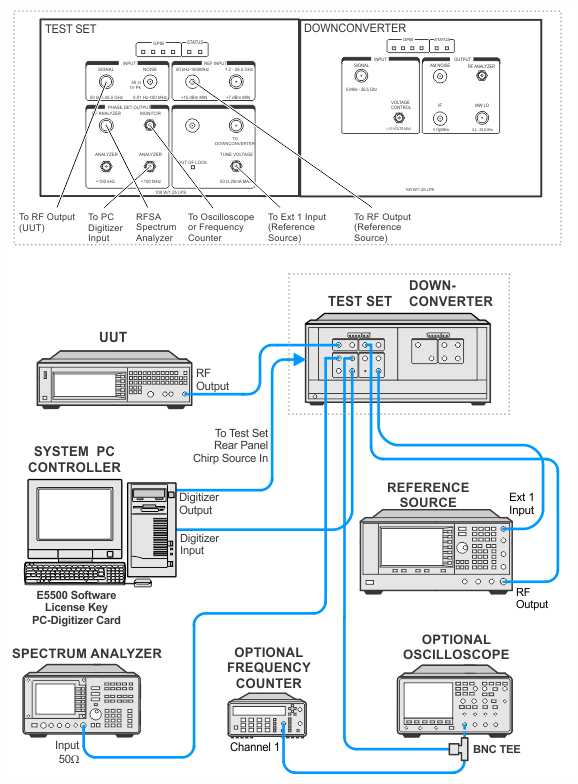
Connect all test equipment as shown.
Connect GPIB cables to all GPIB-controlled test equipment.
Preset all test equipment and the UUT.
In theE5505A Phase Noise System user interface, change the following parameters:
Select the View pull down menu.
Select Display Preferences and un-check the Spurs box.
Select OK to close Display Preferences.
Select the System pull-down menu and select Server Hardware Connections.
Select or ensure that the FFT has NI PCI6111-1, 11 PCI20428W-1, or 89410A selected.
Select Close to close Server Hardware Connections.
Select the Define pull-down menu, select Measurement, and select the following settings:
|
Parameter |
Setting |
|||||||||||||||||||||||||||||||||||
|
Type and Range Tab: |
||||||||||||||||||||||||||||||||||||
|
Measurement Type |
Absolute phase noise (using a phase locked loop) |
|||||||||||||||||||||||||||||||||||
|
Start Offset Frequency |
10 kHz (for standard units or with Option UNX) |
|||||||||||||||||||||||||||||||||||
|
Stop Offset Frequency |
30 kHz (for standard units or with Option UNX) |
|||||||||||||||||||||||||||||||||||
|
FFT Averages |
1 |
|||||||||||||||||||||||||||||||||||
|
FFT Quality |
Custom |
|||||||||||||||||||||||||||||||||||
|
Define Custom Segment Table - FFT Note: the following parameters should be left at their default values for all segments:
|
|
|||||||||||||||||||||||||||||||||||
|
Swept Quality |
Custom |
|||||||||||||||||||||||||||||||||||
|
Define Custom Segment Table - Swept Note: the following parameters should be left at their default values for all segments:
|
|
|||||||||||||||||||||||||||||||||||
|
Sources Tab: |
||||||||||||||||||||||||||||||||||||
|
Carrier Source Connected |
Test Set |
|||||||||||||||||||||||||||||||||||
|
Carrier Source Frequency |
See Table 1 |
|||||||||||||||||||||||||||||||||||
|
Carrier Source Power |
See Table 1 |
|||||||||||||||||||||||||||||||||||
|
Detector Input Frequency |
Same as carrier source frequency |
|||||||||||||||||||||||||||||||||||
|
Reference Source Power |
See Table 1 |
|||||||||||||||||||||||||||||||||||
|
VCO Tune Constant |
Set to 0.1 ppm x Carrier source frequency For example, set to 25 Hz/Volt for a carrier frequency of 250 MHz |
|||||||||||||||||||||||||||||||||||
|
VCO Tune Range |
1 Volt |
|||||||||||||||||||||||||||||||||||
|
VCO Input Resistance |
50 ohms |
|||||||||||||||||||||||||||||||||||
|
Center Voltage |
0 |
|||||||||||||||||||||||||||||||||||
|
Cal Tab: |
||||||||||||||||||||||||||||||||||||
|
Phase Detector Constant |
Measure phase detector constant |
|||||||||||||||||||||||||||||||||||
|
VCO Tune Constant |
Measure VCO tune constant |
|||||||||||||||||||||||||||||||||||
|
Verify calculated phase lock loop suppression |
Blank |
|||||||||||||||||||||||||||||||||||
|
|
|
|||||||||||||||||||||||||||||||||||
|
Block Diagram Tab: |
||||||||||||||||||||||||||||||||||||
|
Carrier Source |
Manual |
|||||||||||||||||||||||||||||||||||
|
Down Converter |
None |
|||||||||||||||||||||||||||||||||||
|
Reference Source |
E8257D |
|||||||||||||||||||||||||||||||||||
|
Phase Detector |
Automatic Detector Selection |
|||||||||||||||||||||||||||||||||||
|
Test Set Tune Voltage Output |
Front Panel |
|||||||||||||||||||||||||||||||||||
|
Test Set Tune Voltage Destination |
Reference Source |
|||||||||||||||||||||||||||||||||||
|
VCO Tune Mode |
DCFM |
|||||||||||||||||||||||||||||||||||
|
Test Set Tab: |
||||||||||||||||||||||||||||||||||||
|
Input Attenuation |
0 dB |
|||||||||||||||||||||||||||||||||||
|
LNA Low Pass Filter |
Auto |
|||||||||||||||||||||||||||||||||||
|
LNA Gain |
Auto |
|||||||||||||||||||||||||||||||||||
|
Minimum Auto Gain |
14 dB |
|||||||||||||||||||||||||||||||||||
|
PLL Integrator Attenuation |
0 dB |
|||||||||||||||||||||||||||||||||||
|
Graph Tab: |
||||||||||||||||||||||||||||||||||||
|
Title |
User specific |
|||||||||||||||||||||||||||||||||||
|
Graph Type |
Single-sideband phase noise (dBc/Hz) |
|||||||||||||||||||||||||||||||||||
|
X Scale minimum |
Same as start offset frequency |
|||||||||||||||||||||||||||||||||||
|
X Scale maximum |
Same as stop offset frequency |
|||||||||||||||||||||||||||||||||||
|
Y Scale maximum |
0 dBm |
|||||||||||||||||||||||||||||||||||
|
Y Scale minimum |
–170 dBm |
|||||||||||||||||||||||||||||||||||
|
Normalize Trace Data to |
1 Hz bandwidth |
|||||||||||||||||||||||||||||||||||
|
Trace Smoothing Amount |
0 |
|||||||||||||||||||||||||||||||||||
Set
the UUT frequency to the first carrier frequency and power in Table
1.
Set the UUT RF Output to On.
Select the Measure pull down menu and select New Measurement.
When the measurement completes, select the Markers icon and place markers at the offsets specified by TME.
|
|
For a 10 Hz offset, the marker will be set to 9.9844 Hz. |
To get these offsets, perform the following steps:
Launch TME with the UUT connected to the test system.
Start the Single-Sideband Phase Noise test.
With the form selected, press Ctrl-A, Ctrl-C on the keyboard to collect the data in the form.
Open an application such as Microsoft Notepad and press Ctrl-V to copy the test point data into this application.
Print out this data and use it to complete this test.
Compare the marker
amplitude value to the specifications from the datasheet shipped with this product (also found with the data collected in step
6).
| If a failure occurs, a three-source measurement should be performed at this carrier frequency and offset to identify a true failure. |
Print out a phase noise plot.
Select the Measure pull down menu and select New Measurement.
Continue to the next carrier frequency and perform the measurement. Note the following frequency specific changes:
At 2 GHz:
Move the reference source RF Output to the 1.2-26.5 GHz REF INPUT from the 50 kHz-1600 MHz REF INPUT.
If this performance test fails, perform the following steps in order:
Check the equipment setup (see above). If the setup is incorrect, make the necessary corrections and rerun the performance test.
Refer to the troubleshooting section of the service guide. If you do not have a printed copy of the service guide (Option OBW), one is available either on the CD-ROM that came with your signal generator shipment or search for your signal generator model number on the Keysight website.
If necessary, obtain service from Keysight Technologies. Refer to Contacting Keysight Technologies.