![]()
All test equipment requires a 30 minute warm-up period to ensure accurate performance.
This manual test verifies that the signal generator's single-sideband phase noise meets specifications.
During this test, a phase noise system is used to measure the single-sideband phase noise of the signal generator. There are four different test setups depending on the carrier frequency being tested:
255 MHz
Go to test setup
600 MHz
Go to test setup
1.0 GHz, 3.2 GHz, 9.6 GHz, and 19.8 GHz
Go to test setup
A Keysight E82X7D Option UNX high performance RF signal generator (reference source) is used to produce carrier frequencies for 255 MHz, 1.0 GHz, 3.2 GHz, 9.6 GHz, and 19.8 GHz. The KeysightN5507A or 70427A downconverter is used to produce a carrier frequency for 600 MHz; this signal is used as the reference source when testing standard models and models equipped with Option UNJ or UNR at 100 Hz, 1 kHz, 10 kHz, and 100 kHz offsets.
|
E8241A |
E8244A |
Test Equipment |
Preferred Model or Alternate Model(s) |
|
X |
X |
Phase Noise System, |
E5505A phase noise system |
|
X |
X |
External Mixer, |
11970A external mixer LO In and IF Out are SMA (f) and connect to APC 3.5 (m) cables. RF In is an SMA (f) but requires an R281A R-Band waveguide which has a 2.4 mm (f) output connector; this is used to connect directly to the RF Output of the signal generator. |
|
|
X |
Adapter, |
R281A R-Band waveguide |
|
X |
X |
Reference Source |
E8247C Opt UNR |
|
X |
X |
Cable, |
8120-4921 |
|
|
X |
Cable, |
8120-6164 |
|
X |
X |
Cable, |
8120-1840 BNC (m)
to (m) cable |
|
X |
X |
Adapter, |
E9625A |
|
|
X |
Adapter, |
11901D |
|
X |
|
Adapter, |
A1250-1749 |
|
|
All test equipment requires a 30 minute warm-up period to ensure accurate performance. |
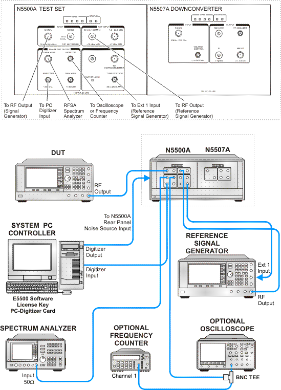
Connect all test equipment as shown.
Connect GPIB cables to all GPIB-controlled test equipment.
Preset all test equipment and the signal generator.
Connect the E82X7D or 866XA RF Output to the N5500A or 70420A Reference Input.
Connect the N5500A or 70420A Tune Voltage Output to the E82X7D Option UNX Ext 1 Input or 866XA EFC.
In the E5504A Phase Noise System user interface, change the following parameters:
Select the ”View” pull down menu.
Select ”Display Preferences” and un-check the ”Spurs” box.
Select "OK" to close Display Preferences.
Select the ”Define” pull down menu, select ”Measurement”, and select the following settings:
|
Parameter |
Setting |
|
|
|
|
Type and Range Tab |
|
|
Measurement Type |
Absolute phase noise |
|
Start Offset Frequency |
1 Hz |
|
Stop Offset Frequency |
10 MHz |
|
FFT Averages |
4 |
|
FFT Quality |
Normal |
|
Swept Quality |
Normal |
|
|
|
|
Sources Tab |
|
|
Carrier Source Connected |
Test Set |
|
Carrier Source Frequency |
255 MHz |
|
Carrier Source Power |
7 dBm |
|
Detector Input Frequency |
255 MHz |
|
Reference Source Power |
10 dBm |
|
VCO Tune Constant |
0.1 ppm x Carrier Frequency for E82X7D; 1.275 Hz/Volt for 866XA |
|
VCO Tune Range |
1 Volt for E82X7D; 10 Volts for 866XA |
|
VCO Input Resistance |
50 ohms for E82X7D; 1E+6 ohms for 866XA |
|
|
|
|
Cal Tab |
|
|
Measure Phase Detector Constant |
Checkmark |
|
Measure VCO Tune Constant |
Checkmark |
|
Verify calculated phase lock loop suppression |
Blank |
|
Phase Lock Loop Suppression |
Use Theoretical Value |
|
|
|
|
Block Diagram Tab |
|
|
Carrier Source |
Manual |
|
Down Converter |
None |
|
Reference Source |
E8257D Asset Control Module (use the E8257C if the E8257D is not available); 866XA |
|
Phase Detector Mode |
Automatic |
|
Test Set Tune Voltage Destination |
Reference Source |
|
VCO Tune Mode |
DCFM for E82X7D; EFC for 866XA |
|
|
|
|
Test Set Tab |
|
|
Input Attenuation |
0 dB |
|
LNA Low Pass Filter |
Auto |
|
LNA Gain |
Auto |
|
PLL Integrator Attenuation |
0 dB |
|
|
|
|
Downconverter Tab |
|
|
Input Attenuation |
Auto |
|
IF Gain |
Auto |
|
Microwave/Millimeter Band |
Microwave (0 – 26.5 GHz) |
|
|
|
|
Graph Tab |
|
|
Title |
User specific |
|
Graph Type |
Single-sideband phase noise (dBc/Hz) |
|
X Scale minimum |
1 Hz |
|
X Scale maximum |
100E+6 |
|
Y Scale maximum |
0 |
|
Y Scale minimum |
-170 |
|
Normalize Trace Data |
1 Hz bandwidth |

Set the signal generator frequency to 255 MHz and the power to 7 dBm.
Set the RF Output to on.
Perform a phase noise measurement.
Select the Measure pull down menu and select New Measurement.
Place markers at the specified offsets.
Compare the marker
amplitude value to the following specifications:
If Option UNJ or UNR fails at
a carrier frequency of 255 MHz and an offset of 1 kHz, it may not be due
to the signal generator. If a failure occurs, a three-source measurement
should be performed at this carrier frequency and this offset
to identify a true failure. (For information on performing a three-source
measurement, refer to the E5505A
phase noise system user documentation.)
|
Offset from Carrier (dBc/Hz) |
|||||
|
|
Standard |
Option UNJ or UNR |
|||
|
Carrier Frequency |
20 kHz |
100 Hz |
1 kHz |
10 kHz |
100 kHz |
|
255 MHz |
-1341 |
-100 |
-124 |
-132 |
-136 |
1. For instruments with serial number prefixes below MY4330 or US4330, the specification is -136 dBc/Hz.
Print out a phase noise plot.
Continue to the next setup and perform the measurement.
|
|
All test equipment requires a 30 minute warm-up period to ensure accurate performance. |
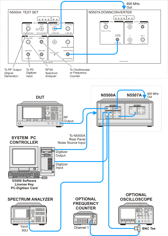
Connect all test equipment as shown.
Connect GPIB cables to all GPIB-controlled test equipment.
Connect the N5507A or 70427A rear panel 600 MHz output to the N5500A or 70420A low frequency Reference Input.
Connect the N5500A or 70420A Tune Voltage Output to the N5507A or 70427A Voltage Control Input.
Set the signal generator frequency to 600 MHz and the power to 7 dBm.
In the E5505A phase noise system user interface, change the following parameters:
|
Parameter |
Setting |
|
|
|
|
Sources Tab |
|
|
Carrier Source Frequency |
600 MHz |
|
Detector Input Frequency |
600 MHz |
|
Reference Source Power |
20 dBm |
|
VCO Tune Constant |
30 Hz/Volt |
|
VCO Tune Range |
10 Volts |
|
VCO Input Resistance |
600 ohms |
|
|
|
|
Block Diagram Tab |
|
|
Down Converter |
System Control |
|
Reference Source |
Manual |
|
Test Set Tune Voltage Destination |
Down Converter |
|
VCO Tune Mode |
DCFM |
|
|
|
|
Downconverter Tab |
|
|
Input Frequency |
600E+6 |
|
Reference Chain Reference |
10 MHz |
|
External Tune Enable |
Checkmark |
|
|
|
|
Graph Tab |
|
|
Title |
User Specific |
The N5507A or 70427A 10 MHz is manually tuned to change the beat note frequency.
Observe the frequency counter and increase/decrease the Tuning Voltage Center value until the beat note frequency is less than the software specified value.
Click the left-mouse button and select the ”Continue” key.
Place markers at the specified offsets.
Compare the marker
amplitude value to the following specifications:
|
Offset from Carrier (dBc/Hz) |
|||||
|
|
Standard |
Option UNJ or UNR |
|||
|
Carrier Frequency |
20 kHz |
100 Hz |
1 kHz |
10 kHz |
100 kHz |
|
600 MHz |
-130 |
-94 |
-118 |
-130 |
-130 |
Print out a phase noise plot.
Continue to the next setup and perform the measurement.
|
|
All test equipment requires a 30 minute warm-up period to ensure accurate performance. |
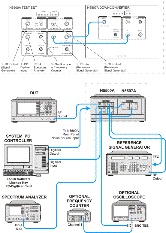
Connect all test equipment as shown.
Connect GPIB cables to all GPIB-controlled test equipment.
Connect the E82X7D or 866XA RF Output to the N5500A or 70420A Reference Input.
Connect the N5500A or 70420A Tune Voltage Output to the E82X7D Ext 1 input or the 866XA EFC.
Repeat the following steps for frequencies of 1.0, 3.2, 9.6, or 19.8 GHz and proceed to "Making the Measurement".
Set the signal generator frequency to either 1.0, 3.2, 9.6, or 19.8 GHz and the power to 7 dBm.
In the E5505A phase noise system user interface, change the following parameters:
|
Parameter |
Setting |
|
|
|
|
Sources Tab |
|
|
Carrier Source Frequency |
1.0, 3.2, 9.6, or 19.8 GHz |
|
Carrier Source Output Connected |
Downconverter |
|
Detector Input Frequency |
1.0, 3.2, 9.6, or 19.8 GHz |
|
Reference Source Power |
10 dBm |
|
VCO Tune Constant |
0.1 ppm x Carrier Source Frequency for E82X7D; (5 E-9) x Carrier Source Frequency for 866XA |
|
VCO Tune Range |
1 Volt for E82X7D; 10 Volts for 866XA |
|
VCO Input Resistance |
50 ohms for E82X7D; 1E+6 ohms for 866XA |
|
|
|
|
Block Diagram Tab |
|
|
Down Converter |
System Control |
|
Reference Source |
E8257D Asset Control Module (use the E8257C if the E8257D is not available); 866XA |
|
Test Set Tune Voltage Destination |
Reference Source |
|
VCO Tune Mode |
DCFM for E82X7D; EFC for 866XA |
|
|
|
|
Downconverter Tab |
|
|
Input Frequency |
1.0, 3.2, 9.6, or 19.8 GHz |
|
|
|
|
Graph Tab |
|
|
Title |
User Specific |
From the Instrument Connections panel, click on ”Optimize Downconverter”.
Perform a phase noise measurement.
Place markers at the specified offsets.
Compare the marker amplitude value to the following specifications:
|
Offset from Carrier (dBc/Hz) |
|||||
|
|
Standard |
Option UNJ or UNR |
|||
|
Carrier Frequency |
20 kHz |
100 Hz |
1 kHz |
10 kHz |
100 kHz |
|
1.0 GHz |
-124 |
-88 |
-112 |
-124 |
-124 |
|
3.2 GHz |
-120 |
-84 |
-108 |
-120 |
-120 |
|
9.6 GHz |
-110 |
-74 |
-98 |
-110 |
-110 |
|
19.8 GHz |
-104 |
-68 |
-92 |
-104 |
-104 |
Print out the phase noise plot.
Continue to the next setup and perform the measurement.
The measurement data must be entered into the following form displayed on-screen when the test is run.
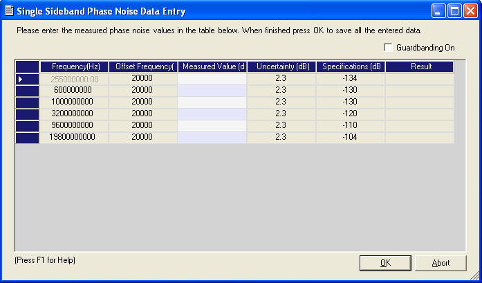
Enter the measured value from the phase noise system into the "Measured Value" column for the appropriate frequency/offset frequency combination. All values must be entered for the test to complete. Entering a measured value and then clicking in the "Result" column in the form will cause the result to appear.
If the "Guardbanding On" checkbox is not selected, then the overall result would not include uncertainty to calculate PASS/FAIL result. Otherwise, the result will be calculated using the displayed uncertainty and will be in the form of PASS/FAIL/INDETERMINATE. The specification against which the measured value is compared is displayed in the "Specifications" column.
If this performance test fails, perform the following steps in order:
Check the equipment setup (see above). If the setup is incorrect, make the necessary corrections and rerun the performance test.
Refer to the troubleshooting section of the service guide. If you do not have a printed copy of the service guide (Option OBW), one is available either on the CD-ROM that came with your signal generator shipment or on the Keysight website.
If necessary, obtain service from Keysight Technologies. Refer to Contacting Keysight Technologies.