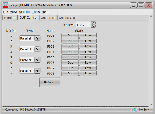
IO Level sets the voltage level of Vout (ST40X Pin No. 9). This level defines the "HIGH" logic level of all I/O pins. The value range is 0.9 to 3.5 V with 0.05 V resolution.
Type selects I/O pin type from Parallel or RFFE for each group. Eight I/O pins are consists of 4 group of 2-pins pair: (Pins No. 1 and 2), (Pins No. 3 and 4), (Pins No. 5 and 6) and (Pins No. 7 and 8).
Name shows the name of assigned signal.
State
When Parallel is selected:
In or OUT - Selects the pin function from Input or Output.
Low or High - shows the current state for input pin. Selects the level from Low or High for output pin
When RFFE is selected:
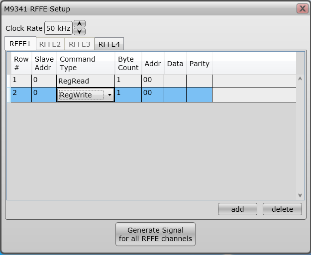
Clicking RFFE setup.. shows the RFFE setup dialog below.
Clock Rate Specifies the clock rate from 25 kHz to 25 MHz. Possible values are 50000/n, with integer n, 2000 to 2.
Row # RFFE command sequence number up to 16
Slave Addr Specifies the slave address in decimal. Slave address should be from 0 to 15 (4 bits).
Command Type Selects the RFFE command sequence type.
Register 0 Write: Register Write by 0
RREad: Register Read
RWRite: Register Write
ERRead: Extended Register Read
ERWRite : Extended Register Write
Byte Count Specifies byte count value in decimal. The value range is depending on command sequence type setting.
Command sequence type |
Byte count range |
Register 0 Write Register Read Register Write |
1 |
Extended Register Write Extended Register Read |
1 to 16 |
Addr Specifies the address value in hex Integer value. The value range is coupled with command sequence type setting.
Command sequence type |
Addr range |
Register 0 Write |
0 (fixed) |
Register Read Register Write |
#h00 to #h1F (0-31) |
Extended Register Write Extended Register Read |
#h00 to #hFF (0-255) |
Data Specifies or reads the data in hex value. Comma separated of data values. The value length is coupled with byte count setting
Parity Shows the parity value for each data.
Generate Signal for all RFFE channels Generates the specified RFFE data for all RFFE channels when this button is clicked.
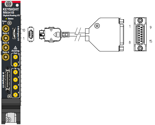
The ST40X-D sub 15 conversion cable is furnished with the M9341B option 001 Interface cables for M9341B
ST40X Pin No. |
D sub 15 Pin No. |
Pin Description |
1 |
1 |
Data 1 |
2 |
2 |
Data 2 |
3 |
3 |
Data 3 |
4 |
4 |
Data 4 |
5 |
5 |
Data 5 |
6 |
6 |
Data 6 |
7 |
7 |
Data 7 |
8 |
8 |
Data 8 |
- |
9 |
N/A |
- |
10 |
N/A |
- |
11 |
N/A |
9 |
12 |
Vout |
- |
13 |
N/A |
- |
14 |
N/A |
10 |
15 |
GND |
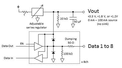
Vout can supply the source up to 100 mA.
This circuit does not sink the current. Hence, when the voltage setting of Vout is changed, it may take time until the voltage reaches the setting value. The following figure shows the circuit diagram of Vout and Data on 8 bit digital I/O.