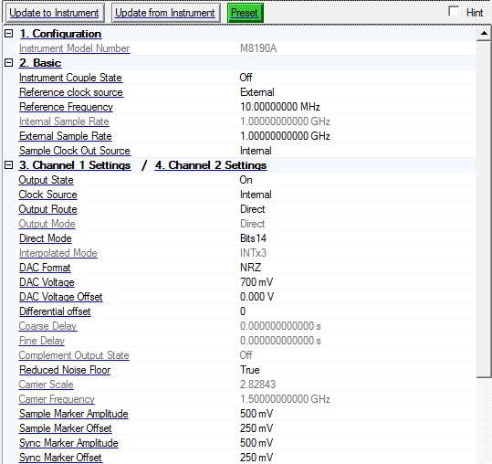
To open the instrument node, click in the tree view. If there is more than one instrument connection, there will be a corresponding number of Instrument listings in the tree view. The figure below shows the Instrument node when connected to an M8190A AWG.
Click this button to send the parameters to the connected M8190A.
Downloading a waveform also updates settings to the instrument.
Click this button to retrieve the parameters from the connected M8190A.
Click this button to set the signal generator to a factory-defined or user-defined state.
Refer to the M8190A user's guide for information on setting a user-defined state.
Displays the model number of the currently connected instrument.
Double-click or use the drop-down menu to enable or disable channel coupling. When enabled, several properties of channel 1 and channel 2 are coupled including: clock source, sample rate, output mode, interpolated mode and others.
Choices: Exernal | Backplane | Internal
Default: External
Double-click or use the drop-down menu to select the M8190A reference source.
External - Use the reference signal provide to the REF CLK IN connector on the M8190A front panel. Be sure to set the reference frequency when external is used.
Backplane - Use the 100 MHz reference provided by the AXIe backplane.
Internal - Use the internal 100 MHz reference.
Range: 1 MHz to 200 MHz
Default: 10 MHz
Enter the frequency of the reference signal applied to the REF CLK IN connector.
Range:
14 Bit Direct Mode 125 MHz to 8 GHz
12 Bit Direct Mode 125 MHz to 12 GHz
Interpolated Mode 1.0 GHz to 7.2 GHz
Default: 1.0 GHz
Display the internal sample clock rate.
This property will be automatically updated by the software. It depends on Symbol Rate, Sample Rate or Bandwidth settings of the carrier, Oversampling Ratio of the waveform and Interpolated Mode of M8190A. At download time, if this property is out of its valid range, software will try to select a new interpolated ratio to fit the range. If it fails to find a proper interpolated ratio, an error message will be reported.
Range:
14 Bit Direct Mode 125 MHz to 8 GHz
12 Bit Direct Mode 125 MHz to 12 GHz
Interpolated Mode 1.0 GHz to 7.2 GHz
Default: 7.2 GHz
Set the external sample clock rate.
Choices: Internal | External
Default: Internal
Select the clock source routed to the SAMPLE CLK OUT connector on the M8190A front panel.
Internal - Route the internal sample clock to the SAMPLE CLK OUT connector.
External - Route the sample clock signal from the SAMPLE CLK IN connector to the SAMPLE CLK OUT connector.
This property is coupled with channel 1 and channel 2 Clock Source when Channel Coupling is enabled.
Choices: Internal | External
Default: Internal
Select the channel sample clock source.
Internal - Use the internal sample clock.
External - Use the external sample clock provided to the SAMPLE CLK IN connector on the M8190A front panel.
Channel 1 and Channel 2 clock sources are coupled when channel coupling is enabled.
Choices: Direct | Interpolated
Default: Interpolated
Select the channel output mode.
Direct - Output a baseband signal.
Interpolated - Output a complex modulated signal at the specified IF frequency. Requires Option DUC.
Channel 1 and Channel 2 output modes are coupled when channel coupling is enabled.
Choices: Bits 12| Bits 14
Default: Bits 14
Double-click or use the drop-down menu to select the channel direct mode.
12 Bit - Set the DAC resolution to 12 bits with a maximum sample rate of 12 GHz. Requires option 12G.
14 Bit - Set the DAC resolution to 14 bits with a maximum sample rate of 8 GHz. Requires option 14B.
Channel 1 and Channel 2 direct modes are coupled when channel coupling is enabled.
Choices: INTx3| INTx12 | INTx24 | INTx48
Default: INTx3
Select the up-sampling ratio used in interpolated mode. The I/Q data is automatically up-sampled to match the DAC sampling rate.
INTx3 - Set the ratio to 3.
INTx12 - Set the ratio to 12.
INTx24 - Set the ratio to 24.
INTx48 - Set the ratio to 48.
Channel 1 and Channel 2 interpolated modes are coupled when channel coupling is enabled or when channel 1 and channel 2 share the same clock source.
Choices: Direct | DC | AC
Default: Direct
Select the channel output route.
Direct - Output is directly from DAC. This has the best IMD performance.
DC - Use the amplified DC output.
AC - Use the amplified AC output.
The AC and DC path share common output connectors on the front panel. The direct DAC path uses different connections on the front panel.
Choices: On | Off
Default: On
Enable or disable the current output state. The current output is determined by the Output Route property.
Choices: On | Off
Default: Off
Double-click or use the drop-down menu to enable or disable the current complement output. The current complement output is determined by the Output Route property.
Choices: RZ | NRZ | DNRZ | Doublet
Default: NRZ
Select the DAC format for this channel.
RZ - DAC returns to zero between each sample. Provides the flattest amplitude response with a 6 dB loss in maximum output power when compared to NRZ.
NRZ- The DAC does not return to zero between samples. Provides higher output power.
DNRZ - Optimized for best NRZ signal using two DACs.
Doublet - The DAC does not return to zero between samples. Provides flatter amplitude response in second Nyquist region. Use this mode when the IF output frequency is greater than 1/2 the DAC sample rate. Dont forget to swap I/Q data to account for spectrum mirroring.
Range:
Direct DAC: 100 mV to 700 mV
DC Output: 150 mV to 1.0 V
AC Output: 200 mV to 2.0 V
Default: 700 mV
Set the peak to peak output voltage.
Range:
Direct DAC: -20 mV to 20 mV
DC Output: -500 mV to 1.0 V
AC Output: Not Applicable
Default: 0 Set the output offset voltage.
The full voltage offset range is coupled to the current Output Voltage and the Output Route values.
Range: determined by calibration
Default: 0
Set the differential amplitude offset in DAC values. The hardware can compensate for little offset differences between the normal and complement output. This property is the offset to the calibrated optimum DAC value, so the minimum and maximum depend on the result of the calibration.
Range:
Sample Rate < 2.5 GHz: 0 to 150 ps
Sample Rate 2.5 to < 6.25 GHz: 0 to 60 ps
Sample Rate ≥ 6.25 GHz: 0 to 30 ps
Default: 0 ps
Set the fine channel delay relative to a trigger or event. In order to compensate for e.g. external cable length differences as well as the initial skew, channel 1 and channel 2 can be independently delayed with a very high timing resolution. The variable delay is the sum of Fine Delay and Coarse Delay. Modifying the variable delay of one channel always affects the delay of the Analog Output AND the Sample Marker of that channel.
This property is configurable only when Reduced Noise Floor is disabled.
Range: 0 ps to 10 ns
Steps:
Sample Rate < 2.5 GHz: 50 ps
Sample Rate 2.5 to < 6.25 GHz: 20 ps
Sample Rate ≥ 6.25 GHz: 10 ps
Default: 0 ps
Set the course channel delay relative to a trigger or event. In order to compensate for e.g. external cable length differences as well as the initial skew, channel 1 and channel 2 can be independently delayed with a very high timing resolution. The variable delay is the sum of Fine Delay and Coarse Delay. Modifying the variable delay of one channel always affects the delay of the Analog Output AND the Sample Marker of that channel.
This property is configurable only when Reduced Noise Floor is disabled.
Choices: On | Off
Default: On
Enable or disable reduced noise floor feature on this channel.
Range: 0 to 12 GHz
Default: 1 GHz
Set the carrier frequency in DUC mode.
Range: 0.0 to 2.82843
Default: 2.82
Set the carrier scale. The carrier scale is used to prevent clipping of the digital data by the DAC. The digital up conversion (DUC) process can generate values that exceed the DAC range. Clipping is prevented by setting the carrier scale to less than the maximum value. Adjusting the carrier scale directly affects the signal output power and dynamic range. Larger values are better until clipping occurs.
Range: 0.0 V to 1.5 V
Set the sample marker output amplitude. Use abbreviations for faster entry (example: 50m = 50 mV).
Set the sampler marker amplitude offset. Use abbreviations for faster entry (example: 50m = 50 mV).
The full voltage offset range is coupled to the current Output Sample Marker Voltage and the Output Route values. For example, when the output route is DC Output ,the minimum offset is (Amplitude/2 -0.5)V, the maximum offset value is (1.75-Amplitude/2)V.
Range: 0.0 V to 1.5 V
Set the sync marker output amplitude. Use abbreviations for faster entry (example: 50m = 50 mV).
Set the sync marker amplitude offset. Use abbreviations for faster entry (example: 50m = 50 mV).
The full voltage offset range is coupled to the current Output Sync Marker Voltage and the Output Route values. For example, when the output route is DC Output ,the minimum offset is (Amplitude/2 -0.5)V, the maximum offset value is (1.75-Amplitude/2)V.