Calibration of BBA channel is very important especially for small signal measurement. For more information, refer to the Keysight MXA Signal Analyzer, Option BBA: Analog Baseband IQ Inputs Technical Overview with Self-Guided Demonstration.
N7614C software only supports MXA and PSA with BBA option available for PAE measurement. As compared to envelope tracking measurement setup, an additional cable connection is needed in the PAE measurement setup so that voltage signals of both ends of sensor resistor are connected to BBA port of signal analyzer with scaling circuits if needed in between.
There are two kinds of hardware setup types:
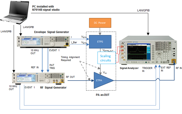
Output of scaling circuits is connected to I Port and I_Bar ( I̅ ) port
Output of scaling circuits is connected to I Port and Q port
Figure 1 shows the first hardware setups with the output of scaling circuits connected to I Port and I_Bar ( I̅ ) port.
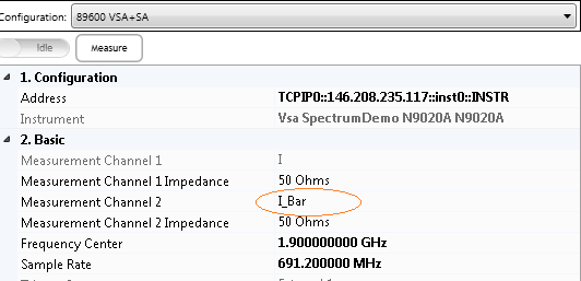
Figure 1. Output of scaling circuits is connected to I Port and I_Bar ( I̅ ) port
Figure 2 shows the second hardware setup with the output of scaling circuits connected to I Port and Q port.
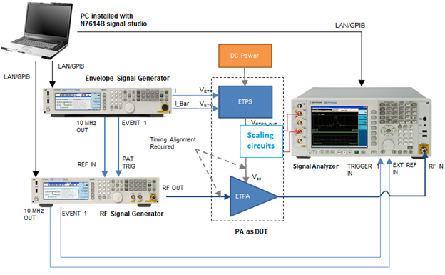
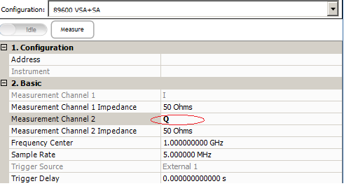
Figure 2. Output of scaling circuits is connected to I Port and Q port
To perform PAE measurement, current of the ETPS output needs to be tested. The N7614C software only supports those models which have a small sensor resistor placed in in the ETPS output path as the current sensor. In such models, current measurement can be done by measuring the voltage dropping on the resistor. Generally, this resistor value must be very small (for example: 0.05Ω) so as to produce less effect on the PA performance. The voltage dropping is measured using the BBA port of signal analyzer which has 14-bit Analog-to-Digital Converter to obtain excellent dynamic range for small signal measurement. Since the maximal input voltage of BBA port of signal analyzer is 1Vpp, additional circuits are needed to process high voltage signal before supplying it as an input to the BBA port.
Generally, scaling circuits are designed in such a way that the voltage dropping, post-processing by the scaling board, can fulfill the BBA channel sensitivity requirement which is about -136dBm/Hz or 300uV/40MHz as shown in the Figure 3.
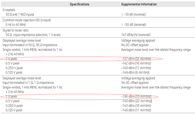
Figure 3. MXA Analog BBA Channel Sensitivity
So, the scaling circuits should be designed in such a way that the sensor resistor has an average dropping voltage greater than 10mV because the minimum ETPS output voltage will be greater than 100mV. Such scaling circuits do not affect the working of the power amplifier as well. Common measurement practices show that the BBA port can measure signals with amplitude greater than several milli-volts. Therefore, you can use high resistor value provided they do not affect the PA performance.
The following two types of typical scaling circuits fulfill the requirement:
If voltages V1 and V2 are greater than 1Vpp, the typical scaling circuit network is as shown in Figure 4.
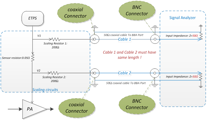
Figure 4. Typical Scaling Circuits 1
Cable 1 and cable 2 must have same length and the input impedance of BBA port must be 50Ω
This scaling circuit network has the following three advantages:
No obvious big capacitive effect like high impedance passive probes
Utilize BBA dynamic range efficiently as compared to normal passive probes which depend on the value of scaling resistor
Low cost and easy to implement as compared to active probes
This model has been verified with ETPS output less than 2Vrms, and current equal to 200mV. You can change sensor resistor and scaling resistor value as per your requirement.
Figure 5 shows the PAE analyzer and measurement settings of the N7614C software for this type of scaling circuits.
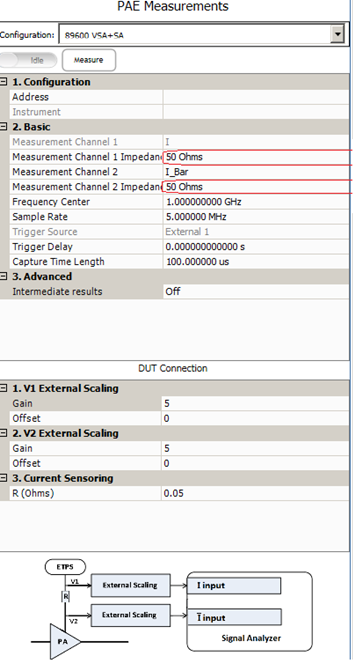
Figure 5. PAE analyzer and measurement settings for Scaling Circuits 1
Gains of the V1 and V2 Scaling can be calculated as follows:
Gain of V1 Scaling=(50Ω+Scaling Resistor 1)/50Ω
Gain of V2 Scaling=(50Ω+Scaling Resistor 2)/50Ω
If voltages V1 and V2 are lower than 1Vpp, the typical scaling network is as shown in Figure 6.
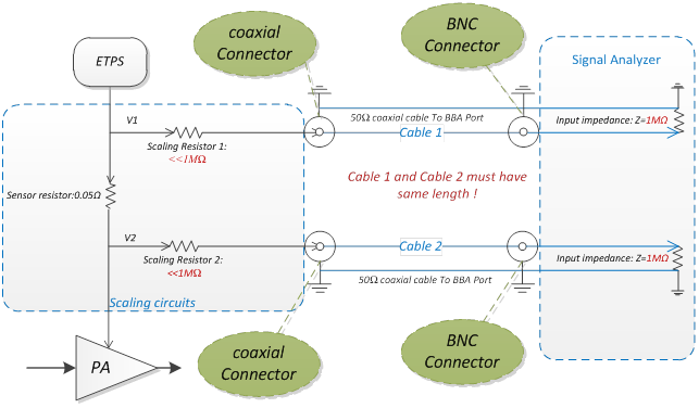
Figure 6. Typical Scaling Circuits 2
Cable 1 and cable 2 must have same length and the input impedance of BBA port must be 1MΩ. The scaling resistor 1 and scaling resistor 2 must be less than 1MΩ.
The input impedance of BBA channel should be 1MΩ and scaling resistor should be very less than 1MΩ (can be directly connected) to achieve 1:1 high impedance passive probe.
Figure 7 shows the PAE analyzer and measurement settings of the N7614C software for this type of scaling circuits.
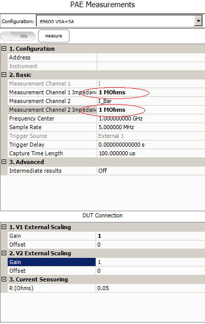
Figure 7. PAE analyzer and measurement settings for Scaling Circuits 2
Gains of V1 and V2 Scaling are:
Gain of V1 Scaling=1
Gain of V2 Scaling=1
MXA/PXA option BBA: Provides Analog Baseband IQ Inputs
MXA/PXA option B25/S40: Provides 25MHz analysis bandwidth or 40MHz analysis bandwidth
89600 VSA Software: Connects the signal analyzer and captures the data for further analysis
Basic VSA option: 89601A/AN-200 (required)
Hardware connectivity option: 89601A/AN-300 (required)
BBA Calibration: BBA function of signal analyzer should be calibrated first before performing PAE measurement. For more information, refer to the Keysight MXA Signal Analyzer, Option BBA: Analog Baseband IQ Inputs Technical Overview with Self-Guided Demonstration.
The table below shows the supported instruments for envelope tracking measurement. For details about the options required for each instrument model, refer to System Requirements.
|
Instrument Type |
Instrument Model Supported |
|---|---|
|
RF Signal Generator1 |
N5182B MXG N5172B EXG N5182A MXG |
|
Envelope Signal Generator |
33522B Arbitrary Waveform Generator 33622A Arbitrary Waveform Generator N5182B MXG N5172B EXG |
|
Signal Analyzer |
N9010A EXA N9020A MXA N9030A PXA |
1. When N5172B EXG/N5182B MXG is used as Envelope Signal Generator, only N5172B EXG/N5182B MXG can be supported as RF Signal Generator.
To set up the measurement system, follow the steps below:
Connect the PC installed with N7614C Signal Studio to the RF Signal Generator, Envelope Signal Generator, and Signal Analyzer through LAN or GPIB.
Connect the frequency reference and trigger for time alignment between Envelope Signal Generator and RF Signal Generator.
If N5172B/N5182B is used as Envelope Signal Generator, connect the 10 MHz Out port of the Envelope Signal Generator to the REF IN port of the RF Signal Generator and connect the EVENT 1 port of the Envelope Signal Generator to the PAT TRIG port of the RF Signal Generator for time alignment of the Envelope Signal Generator output and RF Signal Generator output.
If 33522B or 33622A is used as Envelope Signal Generator, connect the 10 MHz Out port of the Envelope Signal Generator to the REF IN port of the RF Signal Generator and connect the Sync port of the Envelope Signal Generator to the PAT TRIG port of the RF Signal Generator for time alignment of the Envelope Signal Generator output and RF Signal Generator output.
If the RF Signal Generator in use is N5182A MXG, instead of connecting the Sync port of the Envelope Signal Generator to the PAT TRIG port of the RF Signal Generator, you should connect the EVENT 1 port of the RF Signal Generator to the Ext Trig/Gate/FSK/Burst port of the Envelope Signal Generator. Note that in Step 4, EVENT 1 is also connected to the TRIGGER IN 1 port of the Signal Analyzer, so a one-to-two connector needs to be used in EVENT 1 port.
Connect the Envelope Signal Generator output to the ETPS.
If N5172B/N5182B is used as Envelope Signal Generator, connect the I OUT and  OUT of the Envelope Signal Generator to the VETP and VETN port of the ETPS and connect the VETPS_OUT port of the ETPS to the Vcc of the ETPA.
If 33522B or 33622A is used as Envelope Signal Generator, connect the Channel 1 and Channel 2 output of the Envelope Signal Generator to the VETP and VETN port of the ETPS and connect the VETPS_OUT port of the ETPS to the Vcc of the ETPA.
Connect the EVENT 1 port on the rear panel of the RF Signal Generator to the Trigger IN 1 port on the rear panel of the Signal Analyzer using a BNC cable. This is to synchronize the RF Signal Generator and Signal Analyzer in time domain.
Connect the 10 MHz OUT port on the rear panel of the RF Signal Generator to the EXT REF IN port on the rear panel of the Signal Analyzer using a BNC cable.
Connect the RF OUTPUT port of the RF Signal Generator to the input of the PA and connect the output of the PA to the RF INPUT port of the Signal Analyzer.
Connect the scaling circuits into the system.
Connect the measurement point signal of V1 to the BBA I port with scaling circuits in between.
Connect the measurement point signal of V2 to the BBA I̅ port with scaling circuits in between.
PAE measurement can launch a VSA application if no VSA application is online.