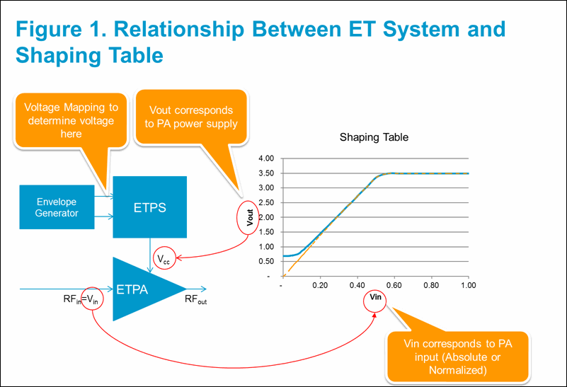
Typically, the shaping table defines the relationship between RF amplitude and the PA supply voltage (Vcc), which is ETPS output voltage. On the other hand, the envelope signal generator generates the signal for ETPS input. Normally, ETPS has some gain and you need to convert ETPS output to input voltage for setting the proper amplitude for the envelope signal generator, using voltage mapping.
Figure 1 shows the relationship between RF, ETPS output (Vcc), and ETPS input voltages.
Figure 1. Relationship Between ET System and Shaping Table (enlarge image)
In the Envelope Tracking Control window, click the block to select a shaping table type from the Transformation Input Type group. Typically, you would select one of the following:
shaping table takes normalized input (from 0 to 1) based on IQ magnitude. It supports shaping at specific RF power level, thus multiple shaping tables need to be switched to support different power level shaping. The shaping input is always scaled to use full scale of shaping table input. (See Figure 2.)
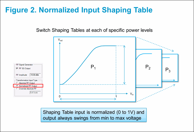
Figure 2. Normalized Input Shaping Table (enlarge image)
based shaping table covers multiple powers with a single shaping table. Depending on the RF power, input power changes the range of shaping table to be used. The shaping table input is in voltage and the Signal Studio software assumes a 50-ohm termination. (See Figure 3.)
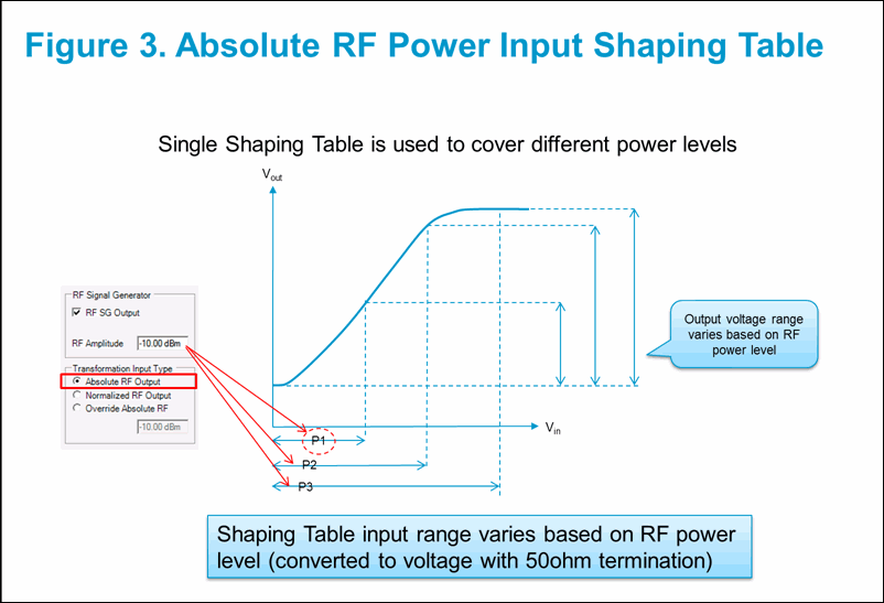
Figure 3. Absolute RF Power Input Shaping Table (enlarge image)
Select shaping table to use in the block.
If you had selected as the Transportation Input Type in Step 1, set the in the block.
In the block, click  ("Generates I/Q and Envelope Waveforms”). This gives you envelope max/min voltage on top of envelope trace.
Populate the yellow cells in the Excel spreadsheet ET Voltage Mapping.xlsx.
Shaping Table Output (Envelope) High/Low
Voffset (REF)
ETPS Gain
If Single Ended ETPS input is used, set “Differential Gain (D4)” to 1.
Enter values from the spreadsheet in the appropriate Envelope Voltage Mapping fields of the block.
Shaping Table Output High (B4) and Low (B5) to Transformed High/Low
Voffset (B6) to Ref and mark the checkbox
"DAC Scale Corrected ETPS Input (Single Ended)" High (H4) and Low (H5) to Mapped High/Low
Vpp (H6) is automatically set in software. No action required.
Common mode voltage (H7) to Vcm
After generating and downloading waveforms, desired envelope Vpp will be shown in the field of the Envelope Signal Generator group.
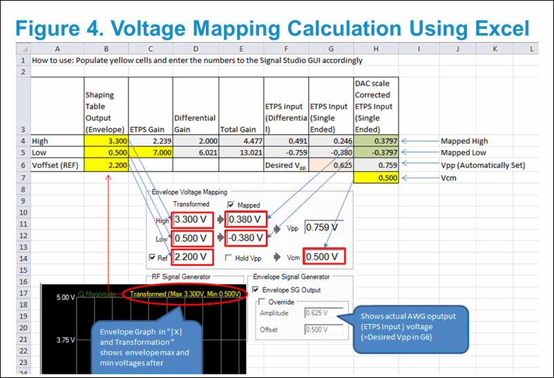
Figure 4. Voltage Mapping Calculation Using Excel (enlarge image)
Reference voltage (Ref) defines how the voltage swings around 0 V in differential output. By default, the reference voltage is set at the middle point of /voltage. If you want to offset the voltage swing, you can override it by marking the checkbox and specify voltage manually.
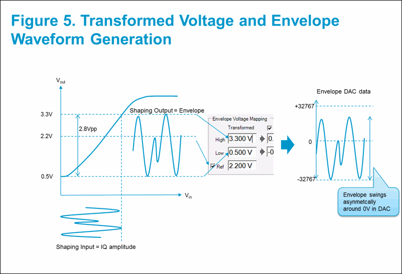
Figure 5. Transformed Voltage and Envelope Waveform Generation (enlarge image)
The voltage parameters are used to determine how the envelope waveform data uses the Arbitrary Waveform Generator’s DAC. Reference voltage corresponds to 0 V DAC. If you override and offset the reference point, the DAC data will not use DAC full scale as shown in Figure 5 above. Since voltage assumes full scale DAC voltage, the actual envelope voltage from AWG will be smaller than . To scale envelope voltage swing to be desired voltage, mapped voltage needs to compensate DAC scaling. The ET Voltage Mapping.xlsx spreadsheet performs DAC scaling correction.
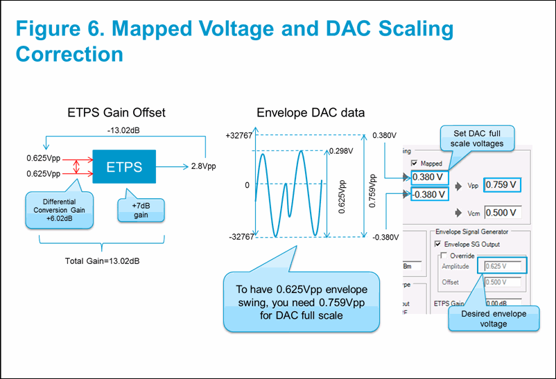
Figure 6. Mapped Voltage and DAC Scaling Correction (enlarge image)
When a normalized shaping table is used, voltage mapping with DAC scaling correction can be done automatically using the following steps:
Select in Transformation Input Type group of the block.
Set / and voltage (Refer to Step 2 above).
Enter gain correction value in to compensate ETPS gain and differential gain (6.02 dB) in dB. If you have 7 dB ETPS gain, your total gain correction is -13.02 dB (=7 dB + 6.02 dB).
Uncheck and check .
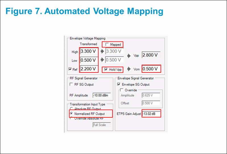
Figure 7. Automated Voltage Mapping (enlarge image)