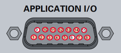
The application I/O can input/output the signals for pulse, noise figure measurements.
Pin |
Factory Default Function |
1 |
Low level Output |
2 |
Low level Output |
3 |
Low level Output |
4 |
Low level Output |
5 |
Low level Output |
6 |
DCOM |
7 |
Pulse generator synchronization trigger input |
8 |
RF pulse modulation input |
9 |
DCOM |
10 |
Pulse Output 1 |
11 |
Pulse Output 2 |
12 |
Pulse Output 3 |
13 |
Pulse Output 4 |
14 |
DCV OFF (+12 V at ON) |
15 |
DCOM |
The function for each pin can be assigned by Interface Control or :CONTrol:SIGNal:AIO:PIN:FUNCtion. (except DCOM)
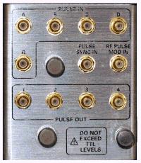
Signal name |
Input/Output |
Description |
PULSE SYNC IN |
Input |
Pulse generator synchronization trigger input |
RF PULSE MOD IN |
Input |
RF source pulse modulation drive input |
Pulse Output 1 (P1) |
Output |
Hardwired pulse train output #1 |
Pulse Output 2 (P2) |
Output |
Hardwired pulse train output #2 |
Pulse Output 3 (P3) |
Output |
Hardwired pulse train output #3 |
Pulse Output 4 (P4) |
Output |
Hardwired pulse train output #4 |
Source port (#S) external switch control output for noise figure |
Output |
Indicates that the source signal is out. This signal is changed to the Low level when the source signal is out. |
Receiver port (#R) external switch control output for noise figure |
Output |
Indicates that noise sweep. This signal is changed to the high level when the target port is used in a sweep for noise measurement. |
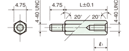
N1966A can be used for the SSA-X. This D connector to RF adapter makes accessing the application I/O signal more convenient.
The following two parts are required to place the N1966A on the E5080B rear panel.
No. |
Description |
Keysight Part Number |
1 |
Standoff-HEX Male-Female 4-40-THD 4.75mm-A/F 9.52mm-LG Brass Ni-Plated |
None |
2 |
Conn Saver Dsub 15POS M-F |
Z2342-37605 |
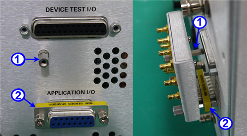
Label on N1966A |
Application I/O connector Pin No. |
Factory Default Function |
A |
1 |
Low level Output |
B |
2 |
Low level Output |
C/R1 |
3 |
Low level Output |
D/R2 |
4 |
Low level Output |
R |
5 |
Low level Output |
PULSE SYNC IN |
7 |
Pulse generator synchronization trigger input |
RF PULSE MOD IN |
8 |
RF pulse modulation input |
1 |
10 |
Pulse Output 1 |
2 |
11 |
Pulse Output 2 |
3 |
12 |
Pulse Output 3 |
4 |
13 |
Pulse Output 4 |
The device test I/O has a capability of two sets of 8 bit I/O and RFFE interface control.
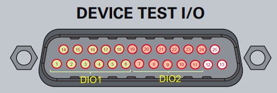
Pin |
Default Function |
1 |
DIO1 Data1 (PIO1) |
2 |
DIO1 Data3 (PIO3) |
3 |
DIO1 Data5 (PIO5) |
4 |
DIO1 Data7 (PIO7) |
5 |
DIO1 Vout |
6 |
DCOM |
7 |
DIO2 Data2 (PIO2) |
8 |
DIO2 Data4 (PIO4) |
9 |
DIO2 Data6 (PIO6) |
10 |
DIO2 Data8 (PIO8) |
11 |
DCOM |
12 |
NC |
13 |
NC |
14 |
DIO1 Data2 (PIO2) |
15 |
DIO1 Data4 (PIO4) |
16 |
DIO1 Data6 (PIO6) |
17 |
DIO1 Data8 (PIO8) |
18 |
DCOM |
19 |
DIO2 Data1 (PIO1) |
20 |
DIO2 Data3 (PIO3) |
21 |
DIO2 Data5 (PIO5) |
22 |
DIO2 Data7 (PIO7) |
23 |
DIO2 Vout |
24 |
DCOM |
25 |
NC |
The function for DIO1 and 2 can be assigned by Interface Control or SENS:CONT:DIO:xxxx commands.
Last modified:
29-Apr-2026 |
New topic |