Last Updated: August 29, 2007
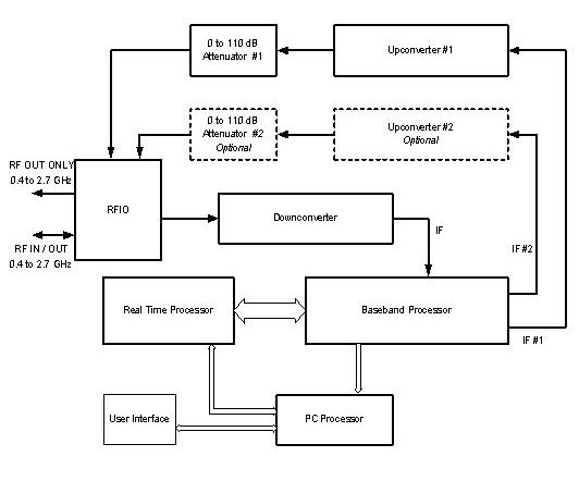
The 0 - 110 dB step attenuator receives its control information from the Upconverter.
Source output level is determined by a combination of three settings that are calibrated during Adjustment:
The IF level from the Base Band Processor.
The 1 dB step attenuator setting in the Upconverter.
The 0 to 110 dB Attenuator setting.
The Motherboard connects all of the subsystems that comprise the E6601A, providing control communication paths, power supplies and rear panel connections.
The Base Band Processor uses FPGAs to generate and capture digital signals. The FPGAs are programmed for the modulation requirements of the application selected.
The Base Band Processor provides the fine resolution frequency and output level control for the Upconverter. An FPGA in the Base Band Processor generates in-phase and quadrature IF signals passed through Digital to Analog Converters which the Upconverter translates to the source output frequency.
The IF from the Downconverter is processed in the Base Band Processor. The analog IF signal from the Downconverter is digitized by an ADC in the Base Band Processor. The digitized signal is sent to the Data Transfer Processor to collect the data before passing it to the HOST/DSP where measurements are made.
Received RF signals pass through the Downconverter where they are mixed down to an IF signal that is sent to the Base Band Processor.
The Downcoverter is designed to remain calibrated over a ± 10 degrees C temperature window. When module temperature drifts outside this window an Alignment is required to generate new calibration coefficients for the Downconverter's current operating temperature.
The 10 MHz Timebase Reference is generated in the Downcoverter module by an oven controlled crystal oscillator. The Reference signal is used in the Upconverter and Downcoverter to synthesize the LO signals as well as the Base Band Processor to synthesize the sample clocks.
The test set can operate with the internal oven controlled crystal oscillator as the Reference or with an external Reference. The test set will lock to an external reference signal of 1, 2, 2.5, 5 or 10 MHz.
The PC Processor module houses the Hard Disk Drive, HOST Processor and the DSP. The PC Processor controls the Manual User Interface, Remote User Interface, Digital Signal Processing (DSP), the Real Time Processor and external peripherals connected to the test set.
The E6601A use a distributed processor control system. The PC Processor receives packets of data or groups of commands from the Real Time Processor, Front Panel Processor and Data Transfer Processor.
Hardware Control Processors on each RF module and the Motherboard control the board and report to the Real Time Processor.
The Front Panel Processor controls the display, backlight and scans the keyboard for inputs.
The Data Transfer Processor located on the Base Band Processor collects measurement data from the receive FPGA on the Base Band Processor and passes it to the HOST Processor for digital signal processing into measurement results.
The RFIO routes signals in and out of the test set and houses the Calibration Power Meter.
The source signal from the Upconverter can be switched to the RF IN/OUT, RF OUT ONLY connectors or looped back to the Calibration Power Meter in the RFIO.
The Calibration Power Meter is calibrated in the factory as the absolute power reference used for source level calibration during an Adjustment of the test set. During Adjustment the output signal is looped back to the Calibration Power Meter in the RFIO.
Once the source signal is calibrated it is used to calibrate the measurement path.
The Real Time Processor is a 400 MHz Power PC processor running a VX-Works operating system.
The Real Time Processor controls Hardware Control Processors on the each of the RF modules and the Motherboard with high level commands. Each Hardware Control Processor uses its own hardware control firmware to set frequency, path and level for that module.
The Hardware Control Processors on each module report to the Real Time Processor during boot up. The Real Time Processor writes those results to the PowerupStatus file during the boot up sequence.
The Upconverter translates the IF signal from the Base Band Processor up to the desired RF output frequency and output level. This signal passes through the 0 to 110 dB Attenuator and the RFIO to get to the RF IN/OUT or RF OUT ONLY ports on the front panel.
The source output frequency is determined by the IF frequency and LO frequency generated in the Upconverter.
The Upconverter controls the steps of the 0 to 110 dB Attenuator.
![]()