Address Table (Multiplexed Mode)
The AUX I/O connector allows the PXB to interface with external equipment by sending and/or receiving supplementary (auxiliary) signaling information, such as:
output markers to an external device from Arbitrary waveform playback sent to external equipment to trigger or respond to waveform changes.
output of signal markers to an external device from real- time signal generation personalities. Signals such as frame markers, pulse- per- second, and even- second, for example, may be supported, depending on the signal generation personality (CDMA, 3GPP, GNSS, LTE, etc.).
input signals from external devices under test to cause the signal generator to modify characteristics of a signal being generated, depending on the signal generation personality (CDMA, 3GPP, LTE, etc.).
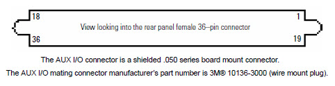
PXBs shipping after May 2013 have a 36-pin female AUX I/O connector and clock circuitry to support strobe functions.
The AUX I/O port is controlled through two groups of settings: global PXB settings (see Global AUX I/O Settings) and application settings (see the real time application's help for specific signal pin assignments).
|
|
The AUX I/O connector supports standard 3.3V TTL signaling levels. Signals support data rates up to 50 MHz with minimum rise and fall times of 3ns. Any pins that are not connected will have a weak pull- up to 3.3V. |
The following table describes the general inputs and outputs accessible through the 36-pin AUX I/O connector. The specific functions controllable by auxiliary signaling vary significantly from one real-time signal generation personality to another. Refer to the documentation for each real-time signal generation personality for additional information.
| Rear-Panel Connector Pin# | RT app UI selection on PXB 2.x SW and later | Input/ Output |
Description |
| 1 | Marker1 | Out | Output marker signal 1 from ARB or Real Time generation, 3.3V |
| 2 | Out | Output marker signal 2 from ARB or Real Time generation, 3.3V (Playback only) | |
| 3 | Marker3 | Out | Output marker signal 3 from ARB or Real Time generation, 3.3V |
| 4 | Marker4 | Out | Output marker signal 4 from ARB or Real Time generation, 3.3V |
| 5 | Out | User clock: Output clock signal from custom real-time mode | |
| 6 | In | AUX strobe: AUX I/O VALID signal supplied by external equipment. Can be configured for positive or negative edge | |
| 7 | Out | 10 MHz reference clock output | |
| 8 | AUX0 | In | AUX Input signal, binary signal, 3.3V |
| 9 | AUX1 | In | AUX Input signal, binary signal, 3.3V |
| 10 | AUX2 | In | AUX Input signal, binary signal, 3.3V |
| 11 | AUX3 | In | AUX Input signal, binary signal, 3.3V |
| 12 | AUX4 | In | AUX Input signal, binary signal, 3.3V |
| 13 | AUX5 | In | AUX Input signal, binary signal, 3.3V |
| 14 | AUX6 | In | AUX Input signal, binary signal, 3.3V |
| 15 | AUX7 | In | AUX Input signal, binary signal, 3.3V |
| 16 | AUX8 | In | AUX Input signal, binary signal, 3.3V |
| 17 | AUX9 | In | AUX Input signal, binary signal, 3.3V |
| 18 | AUX10 | In | AUX Input signal, binary signal, 3.3V |
| 19 | AUX11 | In | AUX Input signal, binary signal, 3.3V |
| 20 | Ground | ||
| 21 | AUX12 | In | AUX Input signal, binary signal, 3.3V See "Address Table" |
| 22 | Ground | ||
| 23 | AUX13 | In | AUX Input signal, binary signal, 3.3V See "Address Table" |
| 24 | Ground | ||
| 25 | AUX14 | In | AUX Input signal, binary signal, 3.3V See "Address Table" |
| 26 | Ground | ||
| 27 | AUX15 | In | AUX Input signal, binary signal, 3.3V See "Address Table" |
| 28 | Ground | ||
| 29 | Out | AUX sample clock, 3.3V, indicates AUX0..AUX15 have been sampled | |
| 30 | Ground | ||
| 31 | Out | AUX out(0) | |
| 32 | Ground | ||
| 33 | Out | AUX out(1) | |
| 34 | Ground | ||
| 35 | Out | AUX out(2) | |
| 36 | Ground |
PXBs that shipped May 2013 or earlier have a 20-pin female AUX I/O connector. The 20-pin connector is compatible with Signal Studio real time applications; however, it doesn't support strobe-related functions.
The AUX I/O port is controlled through two groups of settings: global PXB settings (see Global AUX I/O Settings) and application settings (see the real time application's help for specific signal pin assignments).
![]()
|
|
The AUX I/O connector supports standard 3.3V TTL signaling levels. Signals support data rates up to 50 MHz with minimum rise and fall times of 3ns. Any pins that are not connected will have a weak pull- up to 3.3V. |
The following table describes the general inputs and outputs accessible through the 20-pin AUX I/O connector. The specific functions controllable by auxiliary signaling vary significantly from one real-time signal generation personality to another. Refer to the documentation for each real-time signal generation personality for additional information.
| Rear-Panel Connector Pin# | RT app UI selection in PXB 1.9.x SW | RT app UI selection in PXB 2.x SW | Input/ Output |
Description |
| 1 | AUX1 | AUX0 | In | AUX Input signal, binary signal, 3.3V |
| 2 | Ground | |||
| 3 | AUX4 | AUX3 | In | AUX Input signal, binary signal, 3.3V |
| 4 | AUX6 | AUX5 | In | AUX Input signal, binary signal, 3.3V |
| 5 | AUX7 | AUX6 | In | AUX Input signal, binary signal, 3.3V |
| 6 | AUX9 | AUX8 | In | AUX Input signal, binary signal, 3.3V |
| 7 | Ground | |||
| 8 | AUX12 | AUX11 | In | AUX Input signal, binary signal, 3.3V |
| 9 | AUX14 | AUX13 | In | AUX Input signal, binary signal, 3.3V See "Address Table" |
| 10 | AUX15 | AUX14 | In | AUX Input signal, binary signal, 3.3V See "Address Table" |
| 11 | AUX2 | AUX1 | In | AUX Input signal, binary signal, 3.3V |
| 12 | AUX3 | AUX2 | In | AUX Input signal, binary signal, 3.3V |
| 13 | AUX5 | AUX4 | In | AUX Input signal, binary signal, 3.3V |
| 14 | Ground | |||
| 15 | AUX8 | AUX7 | In | AUX Input signal, binary signal, 3.3V |
| 16 | AUX10 | AUX9 | In | AUX Input signal, binary signal, 3.3V |
| 17 | AUX11 | AUX10 | In | AUX Input signal, binary signal, 3.3V |
| 18 | AUX13 | AUX12 | In | AUX Input signal, binary signal, 3.3V See "Address Table" |
| 19 | Ground | |||
| 20 | AUX16 | AUX15 | In | AUX Input signal, binary signal, 3.3V See "Address Table" |
In Multiplexed Mode, it is necessary to specify an address for AUX IO data for each I/Q channel. These settings are located in the Signal IO node, which is populated by the Signal Studio real time application used in the configuration. See the Signal Studio application's help for more information.
| Decimal | AUX15 | AUX14 | AUX13 | AUX12 | UI Selection |
|---|---|---|---|---|---|
| 0 | 0 | 0 | 0 | 0 | Unassigned1 |
| 1 | 0 | 0 | 0 | 1 | Group 1 |
| 2 | 0 | 0 | 1 | 0 | Group 2 |
| 3 | 0 | 0 | 1 | 1 | Group 3 |
| 4 | 0 | 1 | 0 | 0 | Group 4 |
| 5 | 0 | 1 | 0 | 1 | Group 5 |
| 6 | 0 | 1 | 1 | 0 | Group 6 |
| 7 | 0 | 1 | 1 | 1 | Group 7 |
| 8 | 1 | 0 | 0 | 0 | Group 8 |
| 9 | 1 | 0 | 0 | 1 | Group 9 |
| 10 | 1 | 0 | 1 | 0 | Group 10 |
| 11 | 1 | 0 | 1 | 1 | Group 11 |
| 12 | 1 | 1 | 0 | 0 | Group 12 |
| 13 | 1 | 1 | 0 | 1 | Group 13 |
| 14 | 1 | 1 | 1 | 0 | Group 14 |
| 15 | 1 | 1 | 1 | 1 | Unassigned1 |
1. "Unassigned" means that all baseband boards can respond to
AUX IO data regardless of the first/second address setting of each
BBG.
In firmware versions 1.8.x and 1.9.x, the PXB allowed mixed feedback signals (level triggered and serial signals) and their polarity control. Some applications on PXB need to have this mixed capability for backward compatibility. In firmware version 2.0 and later, the AUX I/O legacy behavior is disabled by default and hidden from view. If your application requires the legacy behavior, you can enable it by doing the following:
| Operating Mode | Input Strobe | Legacy Behavior |
| Dedicated | N/A | No |
| Multiplexed | Free Run | Yes, when the First Address and Second Address are set to “Unassigned” |
| User | No |