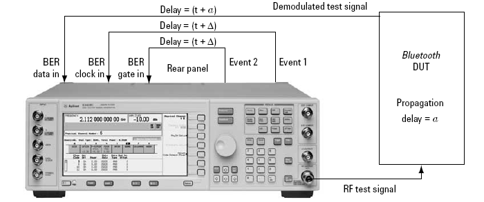
When clock and gate signals generated by the signal source are used to perform BER analysis, it is important to realize that the test signal transmitted by the signal source experiences a propagation delay through the device under test. As a result, the demodulated loopback signal must be realigned in time with the clock and gate signals at the input of the BER analyzer (see figure below). Delay control over the clock and gate signals is provided by the software to enable realignment with the test signal at the input of the BER analyzer.
For BER analysis, the following packet parameters must be set as follows:
any selection (do not use )
If the propagation delay characteristics for the device under test are known, enter the delay value in the clock/gate delay field during waveform configuration. The clock and gate signals associated with the waveform will be delayed by the indicated amount during waveform playback. The resolution of the clock/gate delay parameter is directly coupled to the oversampling ratio setting. It can be determined by dividing the symbol period (1 μs) by the oversampling ratio. To increase the incremental delay resolution, increase the oversampling ratio of the configured waveform. When doing so, remember that increasing the oversampling ratio also increases the projected length of the waveform.
If the delay parameter is unknown, leave the default value (0 μs) in the clock/gate delay field and finish configuring the waveform. After the waveform has been calculated, the clock/gate delay calibration utility can be used to determine the delay characteristics of the device under test.
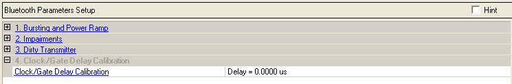
Click  to open the Clock/Gate
Delay Calibration Form, allowing access to additional parameters.
to open the Clock/Gate
Delay Calibration Form, allowing access to additional parameters.