How Gate Charge is Calculated
Gate charge characteristics are generally defined by JEDEC and is used to measure the input charge of gate-controlled power transistors. These include FETs and IGBTs. There is also a standard by IEC.
|
Device types |
Discrete Standard |
Module Standard |
| IGBT, Enhancement, Si | JESD 24-2 | JESD 24-2 |
| FET, Enhancement, Si | JESD 24-2 | JESD 24-2 |
| FET, Enhancement, SiC | New JESD | New JESD |
| FET, Enhancement, GaN, vertical | New JESD | New JESD |
| FET, Enhancement, GaN, Cascode | New JESD | New JESD |
| FET, Enhancement, GaN, eHEMT | New JESD | New JESD |
| FET, Enhancement, GaN, GIT | ||
| FET, Depletion, Si | ||
| FET, Depletion, SiC | ||
| FET, Depletion, GaN, vertical | ||
| FET, Depletion, GaN, Cascode | ||
| FET, Depletion, GaN, eHEMT | ||
| FET, Depletion, GaN, GIT |
This section provides some notes and explains how PD1500A software adapts the JESD 24-2standard or deviates from it. The text focuses on enhancement-mode field effect transistors. It can be used for IGBTs as well.

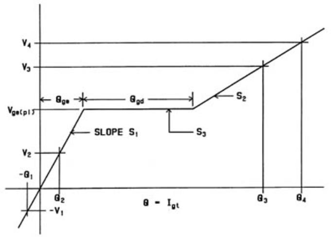
Waveform of gate charge with extraction points according to JESD 24-2
Where:
- Vgs(pl) = voltage where (dvgs)/dt is first minimum during turn-on, last minimum during turn-off
- S1 is linear regression from -Vg(th) to +Vg(th), correlation ≥0.9.
- Qgs=Vgs(pl) /S1
- S2 linear regression using data by gate voltages that assure the device on-state. Correlation ≥0.9
- Qgd=(Vgs(pl) -(Vgs@Q=0))/S2-Qgs

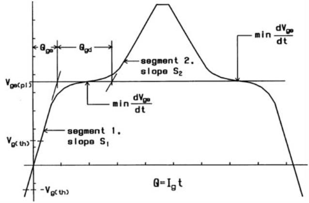
Waveform of gate charge with extraction points according to JESD 24-2
Where:
- Vgs(pl) = voltage where (dvgs)/dt first reaches minimum during turn-on and last minimum for turn-off. Driven with constant Ig conditions
- Qgs = gate charge to reach Vgs(pl) on calculated line segment 1
- Qgd = “Miller” charge: gate charge at Vgs(pl) on calculated line segment 2 minus Qgs
- Qg(th) = gate charge to reach minimum specified gate threshold voltage
- Qg(on) = on-state gate-source charge = charge to reach a gate-source voltage that will support a minimum specified ID(on)
- Qgm = maximum on-state gate-source charge = charge necessary to reach a specified maximum gate-source voltage
- Note: Magnitudes of gate charge and voltage are referred to the coordinate origin (0,0)! Except Qgd
Requirements
- TJ = junction temperature
- ID = on-state drain current
- VDS = off-state drain voltage
- Load impedance as high as practical
- IG = pulsed constant gate current
- Gate charge is measured at a specified gate voltage and is referred to origin (except Qgd)
Notes and Keysight PD1000A deviations (RnD)
- No constant current IG source is used.
- Currently -Vg(th) to +Vg(th) is not specified and not used for linear regression of segment 1
- Cannot be used for depletion mode transistors, how exactly should the standard be adapted for depletion mode or is there another standard for depletion transistors?
- Some Q’s are not yet implemented
- Everything is measured during turn-on, not during turn-off as specified in standard
- Vg(pl) is not value of min(dvg)/dt
- Currently only turn on values from Vg > 0 are used