IV Curve
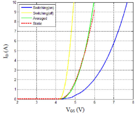
An ID over VDS plot can be directly extracted from plotting ID over VGS for multiple values of VDS. This is done under hard switching conditions with an inductive load, as it is present in a double pulse test. The transistor should be switched very slowly and therefore a large gate resistance should be used. The turn-on and turn-off ID-VGS curves look different. This is among other factors due to the common source inductance LS in the transistor and the abrupt change of ID over time. The two values for the measured gate voltage can be described as  with:
with:
- vgs_onand vgs_off: measured gate voltage during turn-on and turn-off
- Δtr, Δtf: rise and fall time of the drain current
- vi: real gate voltage
- LS: common source inductance
- ΔId: switching drain current
With this, the real gate voltage can be calculated as:  for each output current and output voltage value. These values can then be transferred to an ID-VDS plot for different values of Vgs.This method can also be applied to IGBTs.
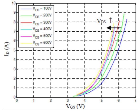
PD1000A software samples ID over Vg during turn-on and turn-off at a certain voltage VDS during turn-on and turn-off and creates the weighted waveform for the real gate voltage. Afterwards values of this graph at certain values for Vg are used to plot points in a ID-VDS plot. With a VDS-sweep the whole IV characteristics can be plotted.

Waveform example of sampling I_d over V_g

Waveforms showing difference between turn-on and turn-off

Graph with I_d-V_g waveforms for multiple V_d
Currently PD1000A software only starts at a gate voltage of 0 V. This is not sufficient to extract the IV-curves for depletion mode transistors. There is only a minor adaption necessary, this is starting the sampling process already for negative values of V_g. Also, Vg/Id sampling seems to be not working properly as sometimes waveforms seem to be incomplete.