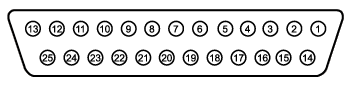
This DB-25 female connector is used to control external test sets. The external test set bus consists of 13 multiplexed address and data lines, three control lines, and an open-collector interrupt line. The Test Set IO is not compatible with the 8753 test sets.
You can change the settings on the External Test Set IO connector through SCPI and COM programming commands. The settings are NOT accessible through the front-panel keys or display menu.
Notes:
The External Test Set pin settings are NOT affected by Instrument State Save/Recall or Instrument Preset.
At PNA Power Up and return from Hibernation, the External Test Set bus data lines, address lines, and control lines are set HIGH, and no strobe lines are pulsed.
Caution: Do not mistake this connector with a Parallel Printer port. A printer may be damaged if connected to this port.
Other System Configuration Topics
|
Pin |
Name |
Description |
|
1 |
Test set select bit 0; tied to GND |
|
|
2 |
TTL input - state may be read with SCPI or COM command |
|
|
3 |
Address and latched data |
|
|
4 |
Address and latched data |
|
|
5 |
Address and latched data |
|
|
6 |
Address and latched data |
|
|
7 |
0V |
|
|
8 |
TTL output Low = Address Strobe |
|
|
9 |
Address and latched data |
|
|
10 |
Address and latched data |
|
|
11 |
Address and latched data |
|
|
12 |
0V |
|
|
13 |
TTL input - state may be read with a SCPI or COM command |
|
|
14 |
CAUTION: Older PNAs have +22v on this line; this will damage a printer. |
|
|
15 |
Test set select bit 1; tied to GND |
|
|
16 |
Test set select bit 2; tied to GND |
|
|
17 |
Address and latched data |
|
|
18 |
Test set select bit 3; tied to GND |
|
|
19 |
Address and latched data |
|
|
20 |
Address and latched data |
|
|
21 |
Address and latched data |
|
|
22 |
Address and latched data |
|
|
23 |
Address and latched data |
|
|
24 |
TTL output - active low data strobe |
|
|
25 |
TTL output - high-read, low write |
Selects addresses of test sets that are "daisy chained" to this port. The select code is set to zero at the PNA connector and is incremented by one as it goes through each successive external test set. Therefore, the first test set in the chain has address zero and so on, for up to 16 test sets.
Connected to ground inside the PNA.
None
Input line used by the test set for holding off a sweep. Holding off a sweep is one way of introducing a delay that allows an external device to settle before the PNA starts taking data. You must write a program that will query the line and perform the delay. The program needs to query the line and keep PNA from sweeping while the line remains low. When a subsequent query detects that the line went high the program would then trigger the PNA to start the sweep.
Use either Single or External trigger mode to control the PNA sweep.
This pin has a series 215-ohms resistor followed by 4.7k-ohm pull-up and then an "ABT" TTL buffered register.
This input is not latched by the PNA hardware. Therefore the input level must be held at the desired state by the test set until it's read by your program.
Thirteen lines are used to output data addresses or input / output data. Several SCPI and COM commands are available for reading and writing to these lines. You can choose to use commands where the PNA provides the appropriate timing signals needed for strobing the addresses and data. Or you can choose to control the timing signal directly. The timing signals are RLW, LAS and LDS. If you decide to do direct control refer to the corresponding SCPI and COM command details. Close attention to detail is needed to insure the desired results.
After a write command, lines AD0-AD12 are left in the state they were programmed. Default setting for Mode is Read / Input).
After a read command, lines AD0-AD12 are left in input mode. While in this mode an external test set attached to the IO is free to set the level on each line.
Each of these I/O pins has a series 215-ohm resistor followed by 4.7k-ohm pull-up resistor.
Write/Read is implemented by an output tri-state TTL buffer / latch for latching and enabling write data in parallel with a TTL input buffer for reading.
Output Address and data setup and hold times are 1us minimum.
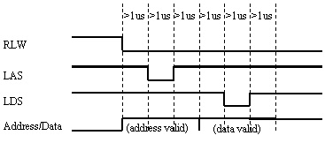
Address & Data I/O Write
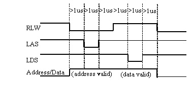
Address & Data I/O Read - Data must be valid for 1us before and after strobe
Two ground pins used as ground references by the test set.
Connected to digital ground.
None.
This line has two behaviors that are command dependent. Refer to the SCPI and COM commands for further details.
In one behavior LAS is one of the lines used by the PNA to provide appropriate timing for writing Address and Data to the Test Set. In this case LAS is controlled automatically by the PNA and is intended to be used as the strobe for the Address. When LAS is low, lines AD0 - AD12 represent the Address. LAS will return to its normally high state when the transaction is finished.
In the second behavior the PNA will NOT provide appropriate timing. In this case LAS is controlled directly by the user through a SCPI or COM command. When the transaction is finished LAS is left set to the state it was programmed to until another command changes it. (Default for LAS is TTL High).
This output pin is driven by a TTL latched buffer with a series 215-ohm resistor followed by 2.15k-ohm pull-up.
Strobe length, setup and hold times are all 1us minimum.
See the description for AD0-AD12 for more timing information.
Query this line with a SCPI or COM command.
This line is a non-latched TTL input, has series 215-ohms followed by 4.64k-ohm pullup.
The Test Set must maintain at the desired TTL level until its read.
WARNING: Early versions of the PNA had +22v on this pin. Connecting a printer to this port will usually damage the printer.
+22V, 100mA max. The 25-pin D connector is the same as a computer parallel printer port connector. Pin (14) corresponds to a printer's "autofeed" line. Connecting a printer to this port will damage the printer if +22v is present since printers requires less than 5V on all control lines.
No connect
None
This line has two behaviors that are command dependent. Refer to the External Test Set IO SCPI and COM commands for further details. (Default setting for LDS is TTL High)
In one behavior LDS is one of lines used by the PNA to provide appropriate timing for writing Address and Data to the Test Set. In this case LDS is controlled automatically by the PNA and is intended to be used as the strobe for the Data. When LDS is low, lines AD0 - AD12 represents Data. LDS will return to its normally high state when the transaction is finished.
In the second behavior the PNA will NOT provide appropriate timing. In this case LDS is controlled directly by the user through a SCPI or COM command. When the transaction is finished the LDS is left set to the state it was programmed to.
This output pin is driven by a TTL latched buffer with a series 215-ohm resistor followed by 2.15k-ohm pull-up.
Strobe length, setup and hold times are all 1us minimum.
See the description for AD0-AD12 for more timing information.
This line is the output for the Read Write signal. It has two behaviors that are command dependent. Refer to the External Test Set IO SCPI and COM commands for further details. (Default setting for RLW is TTL High)
In one behavior RWL is controlled automatically by the PNA during a Read Write operation. When RLW is low, lines AD0 - AD12 represent output Data. When RLW is high, the lines represent input Data.
In the second behavior the PNA does NOT provide the timing. The user must control it directly through the SCPI or COM command. In this case the line is left set to the state it was programmed to.
This pin is a TTL latched output with a series 215-ohm resistor followed by 2.15k-ohm pull-up resistor.
Strobe length, setup and hold times are all 1us minimum.
See the description for AD0-AD12 for more timing information.