If you use separate clocks for the N5102A interface module and the DUT, they must be locked to the same frequency reference. Failure to have a common frequency reference may result in a loss of data.
This cell sets the clock rate at the breakout board side of the N5102A digital interface module. This includes all effects on the clock such as serialization, and interleaving. Because of these settings, the clock rate can be different from the sample rate. The available range for the clock rate depends on the Port Configuration settings and the N5110B software's licensed rate option. For more information, see N5102A Rate Limits.
Changing the Clock Rate or Port Configuration will cause this value to be recalculated.
This cell selects the clock source for the N5102A digital interface. The choices are:
|
Internal |
With this choice, the N5102A digital interface module generates the sample clock. When the clock source is internal, both Reference Frequency and Frequency Reference Source become active. |
|
External |
With this choice, the N5102A digital interface uses a clock provided by an external source through the Ext Clock In connector. The external clock is also available to the DUT at the Ext Clock Out connector. |
|
Device |
With this choice, the DUT provides the clock to the N5102A digital interface through a pin on the breakout board connector ribbon cable. See the N5102A Digital Signal Interface Module Installation Guide for information about breakout boards. |
The connections diagram will update based on this selection. When the Clock Source is Internal, both Reference Frequency and Reference Frequency Source become active.
|
|
If you use separate clocks for the N5102A interface module and the DUT, they must be locked to the same frequency reference. Failure to have a common frequency reference may result in a loss of data. |
This cell selects which clock edge (rising or falling) is aligned with the start of a sample for a parallel or parallel interleaved data transmission, and with the start of each bit for a serial data transmission.
|
Positive |
This choice sets sample alignment to occur on the rising edge of the clock signal. |
|
Negative |
This choice sets sample alignment to occur on the falling edge of the clock signal. The Negative selection functions the same as setting the clock phase to 180 degrees. |
This cell adjusts the clock phase in 90-degree increments to 0, 90, 180, or 270 degrees. The Data Format timing diagram will update to reflect the changed selection.
This cell provides a fine-adjustment for aligning the clock to the valid portion of the data relative to the coarse adjustment associated with the Clock Phase cell. Because this is a fine adjustment, it provides greater benefit at higher clock rates.
The maximum range for this setting is +/- 5 nS, but the actual range depends on the clock rate. The clock skew value will be rounded to a resolution of 1/sample rate. If the sample rate is changed, the clock skew will adjust based on the previous number of samples skewed. The Data Format timing diagram will update to reflect the changed selection.
This setting is only active when the clock rate is greater than 25 MHz.
This cell sets the frequency of the reference used to generate the N5102A's internal clock. This setting is only available when Clock Source is set to Internal and Reference Frequency Source is set to External. When Reference Frequency Source is set to Internal, the value is set to 10 MHz and the cell is disabled.
This cell sets the source of the reference frequency. This setting is only available when Clock Source is set to Internal.
|
Internal |
This setting configures the digital interface to use an internal 10MHz reference. |
|
External |
This setting configures the digital interface to accept an external reference frequency source through the N5101A's Freq Ref connector. |
This cell enables you to select the logic type for the N5102A module data. This selection affects the clock and sample rate ranges. For more information, see N5102A Rate Limits.
|
LVDS |
This choice sets the logic type for the N5102A module to low voltage differential signaling (LVDS). |
|
LVTTL |
This choice sets the logic type for the N5102A module to a low voltage TTL signal. |
|
CMOS 3.3V |
This choice sets the N5102A module logic type to a 3.3 volt CMOS signal. This is the factory preset logic type. |
|
CMOS 2.5V |
This choice sets the N5102A module logic type to a 2.5 volt CMOS signal. |
|
CMOS 1.8V |
This choice sets the N5102A module logic type to a 1.8 volt CMOS signal. |
|
CMOS 1.5V |
This choice sets the N5102A module logic type to a 1.5 volt CMOS signal. |
|
|
Changing the logic type changes the voltage levels. To avoid potential damage to your device or the N5102A module, first verify that the new logic type and voltage are appropriate. |
This cell configures the output/input of the N5102A for Parallel or Serial data transmission. This selection affects the clock and sample rate ranges. For more information, see N5102A Rate Limits.
This cell maps the N5102A's input data format to the output data format. There are two sets of mappings; one for serial and one for parallel. This selection affects the clock and sample rate ranges. For more information, see N5102A Rate Limits.
|
IQ to IQ |
With this choice, samples are transmitted as 16 bits of ’I’ followed by 16 bits of ’Q’; a complete sample is 32 bits or 4 bytes. At the device interface, the 16 ’I’ bits of a sample appear as a serial stream on the I0 line. The 16 ’Q’ bits of a sample appear on the I1 line. Accompanying these two data lines are separate lines for clock and frame signals. The frame signal goes high for one clock cycle during I0 and Q0; for the rest of the sample, the frame is low. |
|
|
|
|
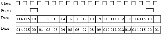
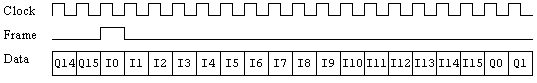
IQ to Sample Interleaved IQ |
With this choice, samples are transmitted as 16 bits of ’I’ followed by 16 bits of ’Q’; a complete sample is 32 bits or 4 bytes. At the device interface, the 16 ’I’ bits as well as the 16 ’Q’ bits of a sample appear as a single serial stream on the I0 line. The ’I’ bits of a given sample precede the associated 16 ’Q’ bits. The frame signal goes high for one clock cycle during the first ’I’ bit of a sample; for the rest of the sample, the frame signal is low. |
|
|
|
|
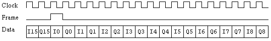
IQ to Bit Interleaved IQ
|
With this choice, samples are transmitted as 16 bits of ’I’ followed by 16 bits of ’Q’; a complete sample is 32 bits or 4 bytes. At the device interface, the 16 ’I’ bits as well as the 16 ’Q’ bits of a sample appear as a single serial stream on the I0 line, with each ’I’ bit preceding the associated ’Q’ bit. The frame signal goes high for one clock cycle during the first ’I’ bit of a sample; during the rest of the sample, the frame signal is low. |
|
|
|
|
IQ to IQ |
With this choice, samples are transmitted as 16 bits of ’I’ followed by 16 bits of Q; a complete sample is 32 bits or 4 bytes. At the device interface, the 16 bits of ’I’ are on the 16 ’I’ parallel lines; the 16 bits of ’Q’ are on the 16 ’Q’ parallel lines. |
|
IQ to Interleaved IQ |
With this choice, samples are transmitted as 16 bits of ’I’ followed by 16 bits of ’Q’; a complete sample is 32 bits or 4 bytes. At the device interface, the 16 bits of ’I’ and the 16 bits of ’Q’ are both on the 16 ’I’ parallel lines. The ’I’ and ’Q’ bits are interleaved, with the ’I’ bits coinciding with the rising edge of the clock, and the ’Q’ bits occurring with the falling edge of the clock. The ’I’ bits for a given sample precede the ’Q’ bits for that sample. |
|
IQ to Interleaved QI |
With this choice, samples are transmitted as 16 bits of ’I’ followed by 16 bits of ’Q’; a complete sample is 32 bits or 4 bytes. At the device interface, the 16 bits of ’I’ and the 16 bits of ’Q’ are both on the 16 ’I’ parallel lines. The ’I’ and ’Q’ bits are interleaved, with the ’Q’ bits coinciding with the rising edge of the clock, and the ’I’ bits occurring with the falling edge of the clock. The ’Q’ bits for a given sample precede the ’I’ bits for that sample. |
|
Real IF to Real IF |
With this choice, samples are transmitted as 16 bits as a real signal; it is not complex, and there is no imaginary part. Typically, this is used to represent a ’real’ IF, but it can be used for any ’real’ signal. Representing the signal by 16 bits allows twice as many samples in the same storage space, and they can be transmitted through the system at twice the rate, compared to 32 bit samples. The samples at the customer interface are also 16 bit samples, and they appear on the 16 parallel ’I’ signal lines. |
This cell sets the polarity of the frame marker that delineates the beginning of each sample during a serial data transmission. This marker shows the start of serial data and may distinguish I from Q data when interleaved. The Data Format timing diagram will update to reflect the changed selection. This feature is only available in serial mode.
|
Negative |
With this choice, the frame line is low while data for the first sample is available. |
|
Positive |
With this choice, the frame line is high while data for the first sample is available. |
This cell delays the frame marker. When there is no frame delay, the frame marker aligns with the 0 bit of the serial data transmission. The range of delay depends on the signal mapping selection. This feature is only available in serial mode. The Data Format timing diagram does not update to reflect frame delay.
This cell sets the binary format for the data values that are transmitted.
|
Two's Complement |
This choice sets the N5102A module data format to a two’s complement representation of the data values. |
|
Offset Binary |
This choice sets the N5102A module data format to an offset binary representation of the data values. |
This cell sets the number of bits in each sample transmitted through the N5102A module. A word is defined as an integer number of bits from 4 to 16. For parallel and parallel interleaved data, word is synonymous with sample. Any unused data lines are driven low. The Data Format timing diagram will update to reflect the changed selection. The word size is coupled with word alignment.
This cell sets the alignment of bits when the word size is less than 16 bits. The Data Format timing diagram will update to reflect the changed selection. This feature is only available in parallel mode.
|
MSB |
With this choice, the most significant bit (MSB) of the data will always be on the same data line and the LSB will move depending on the number of bits in the word. |
|
LSB |
With this choice, the least significant bit (LSB) of the data will always be on the same data line and the MSB will move depending on the number of bits in the word. |
This cell sets the bit ordering of the data that is transmitted through the N5102A module. The Data Format timing diagram will update to reflect the changed selection.
|
MSB |
This selection transmits the most significant bit (MSB) on data line zero for both I and Q for a parallel or parallel interleaved port configuration, and transmits the MSB as the first bit in a sample for a serial port configuration. |
|
LSB |
This selection transmits the least significant bit (LSB) on data line zero for both I and Q for a parallel or parallel interleaved port configuration, and transmits the LSB as the first bit in a sample for a serial port configuration. |
This cell sets the polarity of the I and Q data lines for the N5102A module. The Data Format timing diagram will update to reflect the changed selection.
|
Negative |
With this choice, the data on both the I and Q data lines are inverted. A digital one is represented by a low logic level at the output. |
|
Positive |
With this choice, the polarity of the output data matches the input data. A digital one is represented by a high logic level at the output. |
This cell enables or disables negation of the value of each sample of the I data. Negation changes the affected sample by expressing it in two's complement form, multiplying by negative one, and converting back to the selected numeric format. Negation can be done for I samples, Q samples, or both.
|
On |
With this choice, the I data is negated. |
|
Off |
With this choice, no negation is performed. |
This cell enables or disables negation of the value of each sample of the Q data. Negation changes the affected sample by expressing it in two's complement form, multiplying by negative one, and converting back to the selected numeric format. Negation can be done for I samples, Q samples, or both.
|
On |
With this choice, the Q data is negated. |
|
Off |
With this choice, no negation is performed. |
This cell enables or disables the IQ swap feature.
|
On |
With this choice, the I data is available on the Q data bus and the Q data is available on the I data bus. |
|
Off |
With this choice, I and Q data are not swapped. |