This rectangular 36-pin female connector provides communication signals between the VNA and a material parts handler. You can change the settings on the Material Handler IO connector using SCPI commands.
The M9341A/B I/O module can be work with the PXIe VNA as Material Handler I/O. The input and output interfaces are compatible with ENA and PNA material handler I/O.
Note: On early VNAs this connector is labeled "GPIO". It is covered to indicate that the connector is not functional.
Overview - Controlling a Material Handler
The VNA is capable of interacting with an external material handler or part handler. This allows the VNA to be used in an automated test environment, where devices to be tested are inserted into a test fixture by a part handler, and sorted into pass/fail bins by the handler after testing is complete. By connecting the part handler to the Material Handler I/O ports, the VNA and part handler can synchronize their activities in a way that makes automated testing possible.
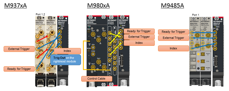
When the M9341A/B I/O module is used with M937xA, M980xA and M9485A, the SMB cables for sync must be connected as shown below.
The M9341A should be placed the following location
M937xA/M980xA: Any slot.
M9485A: Installing at the right side of the rightmost receiver is recommended. When the M9341A is installed between receivers, the sync signal connection is required. The Sync on Port n and Trig on Port (n+1) should be connected with SMB cable when the M9341A is located between Ports n and (n+1).
|
M9341A/B |
M9371A/72A/73A/74A/75A |
M980xA (IO adapter is required) |
M9485A |
|
Sync 1 |
Trig Ready on Port 1,2 module |
Ready for Trigger (IO adapter: Sub/port 3, function assignment is necessary, CONT:SIGN:KDMI:SUB3:FUNC "READY_FOR_TRIGGER" ) |
I/O 1 |
|
Sync 2 |
Trig In on Port 1,2 module |
External Trigger (IO adapter: Sub/port 1) |
Trig on Port 1 |
|
Sync 3 |
Trig Out on the rightmost module |
Index (IO adapter: Sub/port 5, function assignment is necessary, CONT:SIGN:KDMI:SUB5:FUNC "INDEX") |
I/O2 on Port 1 |
|
Number of slot between M9341A/B and VNA module |
SMB Cable Part Number |
Length |
|
1 |
8121-5091 |
120 mm |
|
2 to 3 |
8121-2169 |
165 mm |
|
4 to 8 |
M9485-61605 |
270 mm |
|
More than 9 |
M9485-61604 |
340 mm |
Define the measurements you want to make.
Define limits for each of the measurements.
Configure the VNAs Material Handler port so that it is compatible with your part handler. This usually involves setting the pass/fail logic, pass/fail scope, and pass/fail mode. These settings are made remotely using SCPI commands.
Use a cable to connect the VNA to your part handler.
Put the VNA in External Trigger mode.
Load parts in handler per manufacturer instructions.
Note: The Material Handler configuration settings REMAIN after an Instrument Preset. The settings will revert to their default settings ONLY after the VNA is restarted, or until they are changed by you.
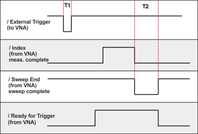
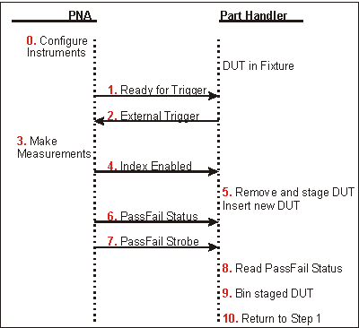
The following diagram and descriptions summarizes the events that occur during automated testing. 'DUT' refers to Device Under Test.
Text Descriptions
(Optional). The VNA sends values out the Material Handler to configure external instruments. The A,B,C, and D ports of the Material Handler can be used to control devices used in testing, such as step attenuators, part handlers, or even the DUT itself. If you wish to use the Material Handler for testing, you will need to write a program to send values out the various lines and ports, as there is no activity on these lines by default.
The part handler receives a Ready for Trigger signal from the VNA. This indicates that the VNA is properly configured and ready to take a measurement.
The part handler sends an External Trigger signal to the VNA. This signals that the part handler has settled, and allows the VNA to begin taking measurements.
The VNA takes measurements on all triggerable channels.
The Index line on the material handler goes to a Low state (default), which means that all required data has been collected by the VNA.
The part handler removes the DUT from the test fixture, and inserts a new DUT into the fixture. This operation is often referred to as part handler indexing. The device just tested is staged (removed from the fixture and prepared for binning), and the next part to be tested is put into the fixture. The removed DUT cannot be assigned to a Pass/Fail bin yet, as the Pass/Fail status is not available.
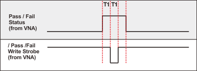
The VNA sends the Pass/Fail Status.
The VNA sends the Pass/Fail Strobe meaning that the Pass/Fail status has been determined.
The part handler reads the Pass/Fail Status line.
The part handler bins the staged part based on the Pass/Fail Status.
The test process repeats at step 1, waiting for Ready for Trigger from the VNA.
Material Handler IO Pin Assignments

|
Pin |
Description |
|
1 |
Ground |
|
2 |
/ INPUT1 |
|
3 |
/ OUTPUT1 |
|
4 |
/ OUTPUT2 |
|
5 |
|
|
6 |
|
|
7 |
|
|
8 |
|
|
9 |
|
|
10 |
|
|
11 |
|
|
12 |
|
|
13 |
|
|
14 |
|
|
15 |
|
|
16 |
|
|
17 |
|
|
18 |
|
|
19 |
|
|
20 |
/ Output port B6 -or (select by command) |
|
21 |
/ Output port B7 or (select by command or dialog box) |
|
22 |
|
|
23 |
|
|
24 |
|
|
25 |
|
|
26 |
|
|
27 |
|
|
28 |
|
|
29 |
|
|
30 |
|
|
31 |
|
|
32 |
|
|
33 |
|
|
34 |
|
|
35 |
|
|
36 |
Input1When this Input line receives a Low pulse from the material handler, data is latched on the OUTPUT1 and OUTPUT2 lines. See OUTPUT1|2 Data Output Write Timing |
|
|
The Input Line activity can be read: |
|
|
SCPI |
|
Output1, Output2See OUTPUT1|2 Data Output Write Timing The current state of these latched TTL outputs may be set High or Low (Default setting) using the (non-user) SCPI put_Output (COM) commands. The next state (following a negative edge on the INPUT1 line) may be pre-loaded to High or Low (Default setting) using the user commands. For example, on the next negative pulse on the INPUT1 line, you want the OUTPUT1 line to go from 0 to 1. To do this: CONT:HAND:OUTP1:DATA 0 'Force the OUTPUT1 line to 0 |
||
|
SCPI |
||
|
Write User Data |
||
|
Read last value written |
||
|
Write non-user data |
||
|
Read last value written |
||
|
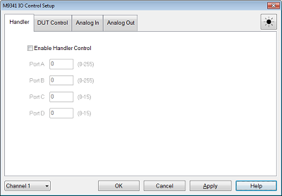
You can specify the port A to D output with this dialog box. The setting value is independent for each channel. These values are set before sweep. Enable Handler Control Enabling the setting for Parts A to D. Port A to D Sends values to the respective Handler I/O port. Although ports C and D are normally bidirectional, ONLY Output mode is allowed using the Interface Control feature. It cannot read from these, or any other, ports |
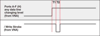
Output Ports A and BThese two general purpose, 8-bit output ports are used to write data to the material handler. When any line changes state, all output lines are latched to the I/O connector as the Output Write Strobe goes Low. The default state for data is Low. |
|
|
Combine to write data to Port F: Ports A and B can be virtually combined to write data to one 16-bit I/O port F. |
|
|
SCPI |
|
Input/Output Ports C and DThese two general purpose 4-bit Input/Output ports are used to write data (Output) or read data (Input). These lines could be used to write to an external device such as a step attenuator. When any line changes state, all output lines are latched to the I/O connector as the Output Write Strobe goes Low. See Data Output Write Timing. |
|
|
Set Input | Output Mode: Each port may be independently defined as Output or Input. |
|
|
SCPI |
|
|
Set Port Logic: The logic for the data lines can be set to either: Positive (1 = High) or Negative (1 = Low). This setting affects all data ports. They cannot be set independently. |
|
|
SCPI |
|
|
Read or write data: Ports C and D can be virtually combined to read or write data to one 8-bit I/O port E. When combined, both C and D ports must be set to either INPUT or OUTPUT mode. |
|
|
SCPI |
|
Port C Status, Port D StatusThese two output lines indicate the Read / Write mode of the C and D ports.
These logic of these status outputs cannot be changed. See Input/Output Ports C and D to learn how to set I/O Mode |
Output Port Write StrobeThis Output line goes Low to write data from Ports A and B and Ports C and D when a change is detected on any of the data lines. These logic of this strobe output cannot be changed. |
External TriggerWhen trigger source is set to external, this Input line accepts a trigger signal from the material handler. This usually means that a part is in place and ready to be tested. |
IndexA Low signal (default) on this Output line indicates to the material handler that the measurement is complete. This usually means that the handler can connect the next device. However, measurement data is not available until data is calculated. See Trigger Timing Diagram. |
|
|
Set Function: This line also serves as a data line. Set the function using the following commands: |
|
|
SCPI |
|
Pass/Fail StateThis Output line indicates to the handler whether the limit test has passed or failed. Pass/Fail state is valid only when the limit test function is ON and while Pass/Fail strobe line is Low. See Pass/Fail Timing Diagram |
|
|
Set Pass / Fail Logic:
|
|
|
SCPI |
|
|
Set Default Conditions:
|
|
|
SCPI |
|
|
Set Pass / Fail Scope:
|
|
|
SCPI |
|
Pass/Fail Write StrobeA Low pulse indicates that Pass/Fail line is valid and the Pass / Fail State is output to the material handler. The Pass/Fail Strobe is fixed in duration and timing. However, when the strobe occurs depends on the Pass/Fail Mode and Pass/Fail Scope (Channel or Global) settings. See Pass/Fail State |
+5V+5V nominal output (100mA max). Protected by self-healing fuse. |
|
|
|
All signals are active low. T1 = 0.1 ms External Trigger pulse width T2 > 10ms Sweep End pulse width (both High and Low) |
|
|
|
T1 = 1 ms Pulse width and response time of Pass / Fail Strobe T2 > 10 ms Ready for Trigger lag |
|
|
|
T1 = 1 ms Write Strobe response time T2 = 1 ms Write Strobe pulse width |
|
|
|
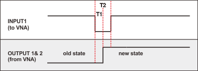
The old state to new state transition can be either low to high (as shown) or high to low. T1 = 0.1 ms Output1|2 response time T2 = 0.1 ms Input1 Strobe pulse width |
Input / Output Electrical Characteristics
All Material Handler I/O Input and Output lines are TTL compatible.
Lines carrying information IN (or bidirectional) to the VNA from the material handler.
|
Maximum Input Voltages: |
-0.5 V to 5.5 V |
|
TTL High level: |
2.0 V to 5.0 V |
|
TTL Low level: |
0 V to 0.5 V |
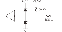
VNA Input and Input/Output Circuit Diagram
|
|
To Handler I/O Port |
Note: The INPUT1 line does NOT have the 10K pullup resistor.
Lines carrying information OUT of the VNA to the material handler.
|
Maximum Output Current: |
-10 mA to 10 mA |
|
|
Output Current |
TTL High level: |
-5 mA |
|
TTL Low level: |
3 mA |
|
|
Output Voltage |
TTL High level: |
2.0 V to 3.3 V |
|
TTL Low level: |
0 V to 0.8 V |
|
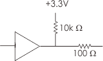
VNA Output Circuit Diagram
|
|
To Handler I/O Port |