83496A/B Clock Recovery Modules
Starting with firmware release A.06.90, 86100D Compatibility mode is no longer being actively tested and supported.
The 83496A is obsolete. The 83496B is discontinued.

Option 100 modules have electrical signals inputs and Option 101 modules have optical inputs. The modules provide continuous, unbanded tuning within the following ranges:
- 50 MBd to 7.10 GBd (83496A/B Standard)
- 50 MBd to 13.5 GBd (83496A Option 200)
- 50 MBd to 14.2 GBd (83496B Option 200)
- 7.10 GBd to 14.2 GBd (83496B Option 201)
Light energy can radiate from the front-panel Data Output connectors on Keysight 83496 modules. The light emitted from this connector is the slightly attenuated light that is input to the front-panel Data Input connector.
The minimum required FlexDCA version for these module in a N1000A is A.06.00 and 86100D is A.02.00.
Maximum electrical signal input for 83496 modules is 6Vp-p differential and 3Vp-p single-ended. Maximum optical signal input for 83496B Option 101 modules is 1.5 mW average and 15 mW peak. Damage will occur at input powers above these levels.
If the display shows a clock recovery lock lost status message, clock recovery cannot be established on the signal. Make sure that your signal is attached with a power level greater than the minimum (see the specifications) and that the symbol rate is set correctly to within the specified acquisition range. Also make sure that the correct source (optical or electrical) is selected.
To use the front-panel clock above 3.2 GBd, 83496 modules require an N1000A-PLK or 86100D-ETR. Or, the front panel output divide ratio must be set on the 83496 to reduce the frequency below 3.2 GHz.
Automatic Relock
If the clock recovery module looses lock, the trigger becomes asynchronous with the data and the instrument will not display a correctly triggered waveform. By default, when lock is lost, the instrument automatically tries to re-establish lock. Automatic relocking is most helpful when probing a device under test. You can turn off or on automatic relocking from the Clock Recovery setup dialog. Loss of lock, or false lock, conditions may be caused by unusual patterns with a large amount of consecutive 1's or 0's. If the module looses lock during any procedure or measurement, reestablish lock and then repeat the procedure or measurement. For example, if lock is lost while saving a pattern waveform to a file, the data stored in the file will be corrupt.
Locking on the Data Rate
When using the module, you must specify the symbol rate of the clock to be recovered and lock the module on the symbol rate. Under two conditions, the module may lock on a symbol rate other than the specified rate. In the first condition, lock can occur if the entered symbol rate is an integer multiple of the actual symbol rate of the signal. The second condition occurs because the acquisition range is broad (greater than ±5000 PPM). This makes it possible for the module to lock on a signal that is higher or lower than the selected value. For example, if you select a 2.48832 GBd symbol rate but the signal is actually 2.5 GBd, the module may still lock on the signal.
Using with Pattern Lock or Jitter Mode
When the instrument is using the pattern lock feature or is in Jitter Mode and the symbol rate is below 400 MBd, the instrument must be triggered from the front panel rather than the 83496's rear-panel connector. Connect the module's front-panel Recovered Clock Out to the mainframe's front-panel Trigger input.
Loop Bandwidth and Jitter
Because jitter is measured relative to the clock, jitter that is present on both the data and the recovered clock can not be detected by the instrument. Jitter that is within the clock recovery module's loop bandwidth appears on the recovered clock. Jitter that is outside of the loop bandwidth does not appear on the recovered clock and can be detected on the data.
Specific jitter frequencies in the vicinity of the loop bandwidth may appear amplified or attenuated due to the scope timebase delay and clock recovery group delay. The optical through-path includes a 40 ns delay line to compensate for the timebase delay. Further compensation can be made, by adding a length of cable between the optical output and the reference receiver input. The electrical through-path does not have a delay line. Compensation can be made, by adding an electrical cable between the electrical output and the vertical channel. However, this may affect signal quality.
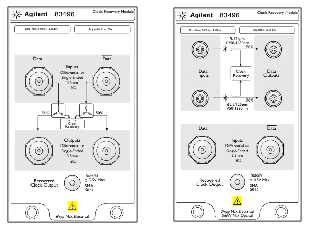
Front-Panel Features
The diagram that is printed on the front panel associates Data Input connectors with Data Output connectors and the internal clock recovery circuit. Data Outputs provide a slightly attenuated input signal for use with a receiver module or other test equipment.
The loop bandwidth of standard modules can be configured at two discrete settings that depend upon the symbol rate. Option 300 modules provide a Golden PLL (tunable loop bandwidth from 15 kHz to over 10 MHz) that meets the requirements for jitter compliance testing to industry standards such as Ethernet and Fibre Channel. Performing a module calibration leaves the module unlocked. Therefore, always lock the module after a calibration. The trigger level is automatically set when using this module.
Figure. Module Front Panels
Electrical Inputs
Two electrical clock recovery inputs are available for single-ended or differential signals. The inputs use 3.5 mm connectors.
Refer to the front-panel annotation and the specifications for information on the maximum input signal level before damage to the module occurs.
The maximum differential electrical signal input is 6 Vpp before damage to the module occurs. The maximum single-ended electrical signal input is 3 Vpp before damage to the module occurs.
Electrical Outputs (Option 100)
The two electrical outputs provide output signals that are attenuated 3 dB from the input signal level. The inputs use 3.5 mm connectors.
Single-Mode Optical Inputs (Option 101)
Use this single-mode (9/125 μm) optical clock recovery input for 1250 nm to 1650 nm signals. The slightly attenuated input signal is available at an associated front-panel output connector. The optical connector includes an adapter that can easily be changed to match the type of connectors that are used on your fiber-optic cables.
The maximum optical input signal is 5 mW before damage to the module occurs.
Multimode Optical Inputs (Option 101)
Use this multimode (62.5/125 μ m) optical clock recovery input for 750 nm to 1330 nm signals. The slightly attenuated optical input signal is available at an associated optical output connector. The optical connector includes an adapter that can easily be changed to match the type of connectors that are used on your fiber-optic cables.
The maximum optical input signal is 5 mW before damage to the module occurs.
Single-Mode Optical Outputs Option 101
The signal available at this single-mode optical Data Output connector is the slightly attenuated signal input on the associated optical Data Input connector. The optical connector includes an adapter that can easily be changed to match the type of connectors that are used on your fiber-optic cables.
Light energy can radiate from the front-panel Data Output connectors on Keysight 83496 modules. The light emitted from this connector is the slightly attenuated light that is input to the front-panel Data Input connector.
Multimode Optical Outputs Option 101
The signal available at this multimode optical Data Output connector is the slightly attenuated signal input on the associated optical Data Input connector. The optical connector includes an adapter that can easily be changed to match the type of connectors that are used on your fiber-optic cables.
Light energy can radiate from the front-panel Data Output connectors on Keysight 83496 Option 101 modules. The light emitted from this connector is the slightly attenuated light that is input to the front-panel Data Input connector.
Recovered Clock Output
This front-panel SMA connector provides an auxiliary recovered clock output for triggering the instrument (via the front-panel trigger) when using pattern lock or Jitter Mode with clock rates less than 400 MBd. Also use this output to trigger other test equipment such as Bit Error Ratio Testers. The output is a full rate clock for symbol rates up to 7.1 GBd and a half rate clock for higher symbol rates.
To configure clock recovery
- Connect the data signal to the clock recovery module's data input connector.
- Connect the clock recovery module's data output to the receiver module's data input connector.
-
 Press the Trigger button located at the bottom of the application. In the dialog box's General Trigger Setup tab, select for the Source:
 - Left Module or Right Module (dependent upon the module position). This specifies triggering the instrument via the recovered clock on the module's rear-panel connector.
- Front Panel. Connect the module's front-panel Clock Out to the instrument's Trigger input connector. The trigger level is automatically set when using this module.
-
 Click the CDR button that is located on the bottom of the application. Or, click Setup > Clock Recovery Setup. This opens the clock recovery setup dialog.
 - In the Clock Recovery Setup dialog box, select the Source from the list. Select the Data Rate and the Loop Bandwidth.
Option 101 modules: Light energy can radiate from the front-panel Optical Output connector. The light emitted from this connector is the slightly attenuated light that is input to the front-panel Optical Input connector.
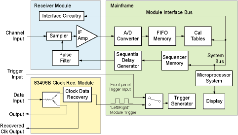
Simplified Block Diagram
Figure. Example Block Diagram with Clock Recovery Module