Clock Recovery Module Setup
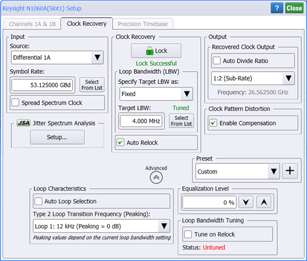
Use this Clock Recovery Setup dialog to configure modules with clock recovery. This includes the N1092A/B-CDR, N1060A, N107x-series, 86108A/B, and 8349x-series modules. The available fields in the dialog depend on the type of clock recovery module used. When configuring clock recovery for a Precision Waveform Analyzer (N1060A and 86108A/B), this dialog includes channel and precision timebase tabs. If clock recovery unlocks, the Clock Recovery Lock Lost dialog is displayed only if Auto Relock is enabled.
The light emitted from the N1077A, N1078A, 83496A/B, 8349x-series modules with optical Data Out connectors is the slightly attenuated light that is input to the front-panel Data In connectors.
Input Fields
Source
Use the Source field to set the source for clock recovery, which vary depending on the clock recovery module. For example, N1076A/B extended modules have electrical inputs while N1078A extended modules have both electrical and optical inputs. Modules with optical inputs may use multimode or single-mode connectors as described in the module's topic within this help system.
Input Enable High Gain (N1078A)
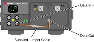
For N1078A modules only, if clock recovery fails to lock on an optical signal, the output from the module's internal O/E converter may need to be amplified. Select Enable High Gain and the signal is internally amplified after it has entered the N1078A's Data In + electrical input connector. To protect the N1078A, observe all cautions in this section. This feature is only displayed when an N1078A is connected and is only available when an optical input source is selected.
The supplied jumper cable must always be connected when Enable High Gain is selected as shown in this picture.
To turn Enable High Gain on:
- Connect the jumper cable.
- Select an optical Input Source.
- Select Enable High Gain.
To turn Enable High Gain off:
- Clear Enable High Gain, or
select an electrical Input Source, or
press Setup > Default Setup. - Remove the jumper cable.
Never exceed 8 mW (option S50) or 4mW (opton SXT) optical input signal power at the N1078A's optical Data In connector regardless of the state of the Enable High Gain setting. Failure to observe this caution will result in damage to the N1078A.
Before selecting Enable High Gain, always connect the supplied semi-rigid jumper cable between the N1078A's Data Out and Data In + connectors. Failure to observe this caution may result in damage to the N1078A.
Always clear Enable High Gain before disconnecting the supplied semi-rigid jumper cable between the N1078A's Data Out and Data In + connectors. Failure to observe this caution may result in damage to the N1078A.
When Enable High Gain is selected, never connect an electrical cable to the N1078A's Data In + connectors except for the supplied semi-rigid jumper cable which connects the N1078A's Data Out and Data In + connectors. Failure to observe this caution may result in damage to the N1078A.
Enable High Gain is only displayed in the dialog when an N1078A is connected and is only active when an optical source is selected.
Symbol Rate
Enter the Symbol Rate of the signal directly, or click Select From List to select from a list. Since the loop bandwidth capture range is wider than the selected symbol rate, it is possible for the module to lock on a signal that is higher than the selected value. For example, if you select a 2.48832 GBd symbol rate but the signal is actually 2.5 GBd, the module may still lock on the signal.
Spread Spectrum Clock Field
FlexDCA uses the average symbol rate to recovery the clock. However, when performing clock recovery on a Spread Spectrum Clock (SSC) signal, using the nominal symbol rate may be required. When Spread Spectrum Clock is selected, the nominal rate is used.
NRZ / PAM4
Specifies the signal type (NRZ or PAM4) that selects that calibration factors for NRZ or PAM4 signals be applied to either:
- Option JSA phase detector gain correction with N1092A/B-CDR, N1060A, N1076A/B, N1077A, N1078A, or 86108B option JSA modules.
- Option CDR phase detector gain correction with N1092A/B option CDR modules that have been programmed with custom NRZ and PAM4 calibration factors.
Clock Recovery Fields
After making your selections, click the Lock button at the top of the Clock Recovery field to lock the clock recovery.

Loop Bandwidth (LBW)
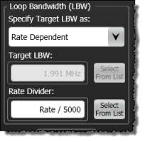
Use the Loop Bandwidth fields to configure the bandwidth of the clock recovery's phase locked loop. Because jitter is measured relative to the clock, jitter that is present on both the data and the recovered clock cannot be detected by the instrument. Jitter that is within the clock recovery module's loop bandwidth appears on the recovered clock. Jitter that is outside of the loop bandwidth does not appear on the recovered clock and can be detected on the data. For this reason, you can select the loop bandwidth for the clock recovery module. The available loop bandwidth settings depend on the module as shown in the following table. Fixed values are entered in Hertz; rate dependent values are expressed as a symbol rate ratio (LBW = rate/n). The selected bandwidth applies both to the recovered clock and to the front-panel Recovered Clk Output. You can also adjust the equalization level on the PLL loop characteristics for clock recovery as explained in Equalization Level later in this topic.
Auto Relock
Select Auto Relock to enable automatic signal re-locking while circuit probing. This feature frees you to concentrate on handling the probe rather than locking the instrument.
| Module | Available Loop Bandwidth Setting | |||
|---|---|---|---|---|
| Fixed | Rate Dependent | Low (270 kHz) |
High (1.5 MHz) |
|
| N1060A | ■ | ■ | ||
| N1078A | ■ | ■ | ||
| N1077A | ■ | ■ | ||
| N1076B | ■ | ■ | ||
| N1076A | ■ | ■ | ||
| N4877A | ■ | ■ | ||
| 83496A/B Option 300 | ■ | ■ | ||
| 83496A/B Standard | ■ | ■ | ||
Clock Pattern Distortion
Turns Clock Pattern Distortion Compensation on or off. Clock Pattern Distortion Compensation compensates for coupling between the pattern and the recovered clock. FlexDCA automatically turns this setting on under the following situations:
- Keysight CDR hardware
- DCA-M or N1000A DCA-X timebase/sampling hardware used.
- Pattern locked with “Acquire Entire Pattern” selected.
It is recommended that you not change this setting unless performing a cross correlation.
Requires active support subscription for MFG or RND package license with F-PCOM feature (date 2022.0615).
Requires FlexDCA revision A.07.00 and above.
Output Fields
Recovered Clock Output
Select Auto Divide Ratio for automatic selection of the clock divide ratio that is applied to the front-panel recovered clock output. Available divide ratios vary depending on the symbol rate. With manual selection, select the divide ratio from available settings in the drop-down list.
Aux Clock Output (N1092A/B-CDR, N1076A/B, N1077A, N1078A DCA-M)
For N107x-series DCA-M clock recovery modules, the auxiliary clock divide output ratio and frequency of the front-panel Aux Clock Output is displayed.
Trigger on Data (83496A/B modules)
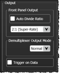
On 83496A/B modules, select Trigger on Data when triggering on data instead of recovering the clock. The data is passed to the rear panel via an AC coupled limit amplifier. Symbol rate and loop bandwidth settings are not adjustable. Triggering on the data is similar to not having a clock recovery module and using a splitter to divide the input signal and routing one portion to the front-panel trigger input. While triggering on the data provides a quick method of checking the data waveform, be aware that the displayed response may be missing 75% of the data patterns. This happens because triggering occurs at either the 1-to-0 or 0-to-1 data transition, and as a result the instrument will only be triggered when a transition occurs in the data instead of triggering on any symbol period as with a clock. For example, consider a pattern such as 1111000. Only the transition between the 1-to-0 triggers the instrument. Transitions between adjacent lows and highs will not cause trigger events. The recovered clock will still be available at the front-panel Recovered Clk Out even when set to trigger on the data.
The Trigger on Data selection is grayed out and is not available for the N4877A module.
JSA Jitter Spectrum Analysis Field
Click Setup to configure jitter spectrum analysis, which is available in FlexDCA's Oscilloscope, Eye/Mask, and Jitter Modes.
Requires an N1060A, N107x-series clock recovery module, or 86108A/B module with Jitter Spectrum Analysis and SW Clock Recovery Emulation.
Advanced Settings
 Click the expander arrow at the bottom of the dialog to view advanced settings, which provide additional control of the clock recovery loop dynamics. The purpose of clock recovery is to extract a clock from the incoming data signal and to provide the DCA with a trigger that is synchronous with the data signal. The clock recovery loop bandwidth primarily determines how well the recovered clock tracks low-frequency jitter on the input signal.
Type 2 Loop Transition Frequency (Peaking)
Some signals have very large low-frequency jitter from either extremely dirty clocks or intentional modulated clocks such as found in SSC (spread spectrum clocking). In this case the clock recovery system provides additional control of the loop dynamics allowing you to select the loop's Type-2 Transition Frequency.
The Type-2 Transition Frequency indicates the frequency below which the second integrator in the loop starts to provide extra gain. Increasing this frequency provides additional loop gain and improves the tracking of the loop. The following figure shows the jitter multiplier as a function of jitter frequency for a loop-bandwidth setting of 5 MHz and various settings of transition frequency. This multiplier is the magnitude of the observed jitter transfer function (OJTF). This additional tracking also increases the peaking in the closed-loop jitter transfer function (JTF). Calculated values of the peaking are provided in the user interface next to the available selections for Type-2 Transition Frequency.
Figure. OJTF for 5 MHz LBW vs. Type-2 Transition Frequency
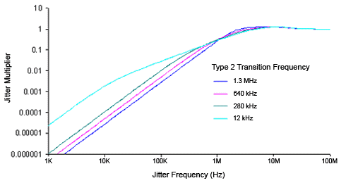
The Type-2 Transition Frequency is automatically coupled to CDR loop bandwidth in normal operation (Auto is selected) and provides the desired loop characteristic for most measurements. The current setting is displayed in the Type 2 Loop Transition Frequency (Peaking) list. To override the automatic selection, unselect Auto and select an available Type-2 Transition Frequency value:
- 12 kHz (available for all loop bandwidths)
- 280 kHz (available for loop bandwidths > 600 kHz)
- 640 kHz (available for loop bandwidths > 1.6 MHz)
- 1.3 MHz (available for loop bandwidths > 4.5 MHz)
The Advanced settings are available for the N107x-series DCA-M modules, 86108A/B modules, and the N4877A extended module. The Advanced settings are not shown for 83496A/B modules.
Equalization Level
The Equalization Level setting fine tunes the equalization level on the PLL loop characteristics for clock recovery. The default value is 0%. The range can be set from 0% to 100% in increments of 1%.
Loop Bandwidth Tuning

When locking clock recovery, Loop Bandwidth Tuning increases the accuracy of the Target LBW (Loop Bandwidth) setting. Loop bandwidth tuning calculates the loop gain on live input data to arrive at an improved loop bandwidth setting. This feature is recommended when performing measurements that are sensitive to loop bandwidth, such as TDECQ.
When Tune on Relock is selected, loop bandwidth tuning is selected to be appended to the normal clock recovery relock algorithm. In other words, when you select Tune on Relock, loop bandwidth tuning is not applied until the next time that clock recovery is relocked. Click the Clock Recovery Lock button at the top of the dialog to initiate a relock. Enabling this setting increases the time needed for the clock recovery to lock. For example, it could add an additional 3 or 4 seconds when locking the clock recovery. By default, Tune on Relock is turned off.
In the following situations, Loop Bandwidth Tuning may not result in reliable adjustment in which case, turn off this feature:
- Degraded input signals
- Low-amplitude input signals
When clock recovery is locked, changes to any of the following loop bandwidth settings will invalidate the loop bandwidth tuning and the tuning status will become untuned:
- Target LBW setting
- Loop characteristics (peaking)
- Equalization Level setting
- Enable High Gain setting (N1078A DCA-M with optical input data)
Presets
Presets allow you to save your dialog settings to a setup file. Recall a preset to instantly configure your clock recovery to your specification. You can save as many presets as you need. The Preset list shows all of the factory provided presets as well as any that you have created. If you scroll to the end of the list and click the <Edit List> entry, the Edit Clock Recovery Presets List dialog opens which allows you to reorder, delete, or rename items in the list. In the list, the names of factory provided presets includes the text (factory) which indicates that the entry cannot be edited.
- To save your settings, click the
 button.
 - To recall your settings at a later date, click Load.
Keysight Supplied CDR Presets
- CEI-28G-SR
- CEI-28G-VSR/MR
- CEI-56G-VSR/MR/LR (26 GBd)
- CEI-112G-VSR/MR/LR (53 GBd)
- IEEE 100G-KR4_CR4
- IEEE 10G-KR_40G-KR4
- IEEE 40G-CR4_100G-CR10
- IEEE 802.3bs/cd (26 GBd) NRZ (Covers the IEEE 802.3cu clause)
- IEEE 802.3bs/cd (26 GBd) PAM4 (Covers the IEEE 802.3cu clause)
- IEEE 802.3bs/cd/ck (53 GBd) (Covers the IEEE 802.3cu clause)
- Infiniiband EDR
- PCI Express Gen 3
- SATA Gen 1
- SATA Gen 2
- SATA Gen 3
- USB 3.0 Gen 1
- USB 3.0 Gen 2