83496A Module Specifications
83496A module specifications and characteristics apply when a module is installed in the instrument mainframe. The following notes refer to the module specifications listed in this chapter.
All specifications describe warranted performance over the temperature range +10° C to + 40° C (unless otherwise noted). The specifications are applicable after the temperature is stabilized, which occurs after 1 hour of continuous operation and while module calibration is valid. Many performance parameters are enhanced through frequent, simple user calibrations.
Specifications describe warranted performance. Characteristics provide useful, nonwarranted information about the functions and performance of the instrument. Characteristics are printed in green italics.
Factory Calibration Cycle. For optimum performance, the instrument should have a complete verification of specifications once every 12 months.
Nominal Value indicates the expected, but not warranted, value of the parameter.
| Item | Description |
|---|---|
| Use | Indoor |
| Temperature | |
| Operating Non-operating |
0 °C to +55 °C
–40 °C to +70 °C |
| Altitude | |
| Operating | 4600 m (15,000 ft) |
| Non-Operating | 15,300 m (50,000 ft) |
| Humidity | |
| Operating Non-Operating |
Up to 90% relative humidity at < 35 °C
Up to 90% relative humidity at < 35 °C |
| Net weight | Approximately 1.2 kg (2.6 lb) |
| Shipping weight | Approximately 2.1 kg (4.6 lb) |
| Power requirements | Supplied by mainframe |
| Channel Type | Differential or single-ended electrical |
| Maximum Input (characteristic) | |
| Electrical (ac coupled) | 6 Vpp differential
3 Vpp single-ended |
| Data Rates | |
| Standard Option 200 |
50 Mb/s – 7.1 Gb/s continuous tuning. 50 Mb/s – 13.5 Gb/s continuous tuning. |
| Output Random Jitter (RMS), Internal Recovered Clock Trigger | |
| 50 Mb/s – 4.2 Gb/s: | < 3 mUI 700 fs (0.9 mUI) at 1.25 Gb/s, characteristic) |
| 4.2 Gb/s – 7.2 Gb/s: | < 700 fs (400 fs at 4.25 Gb/s, 500 fs at 2.5 Gb/s, characteristic) |
| 7.2 Gb/s – 11.4 Gb/s: | < 500 fs (300 fs at 10 Gb/s, characteristic) |
| 11.4 Gb/s – 13.5 Gb/s: | < 700 fs |
| Verified with PRBS7 pattern, electrical inputs > 150 mVp-p to acquire lock. Output jitter verification results of the 83496A can be affected by jitter on the input test signal. | |
| The 83496A will track jitter frequencies inside the loop bandwidth, and the jitter will appear on the recovered clock output. Vertical noise on the input signal will be converted to jitter by the limit amplifier stage on the input of the clock recovery. These effects can be reduced, by lowering the loop bandwidth setting. | |
| Output Random Jitter (RMS), Front Panel Recovered Clock | |
| 50 Mb/s – 4.2 Gb/s: | < 4 mUI 700 fs (0.9 mUI) at 1.25 Gb/s, characteristic) |
| 4.2 Gb/s – 7.2 Gb/s: | < 900 fs (400 fs at 4.25 Gb/s, 500 fs at 2.5 Gb/s, characteristic) |
| 7.2 Gb/s – 11.4 Gb/s: | < 700 fs (300 fs at 10 Gb/s, characteristic) |
| 11.4 Gb/s – 13.5 Gb/s: | < 900 fs |
| Verified with PRBS7 pattern, electrical inputs > 150 mVp-p to acquire lock. Output jitter verification results of the 83496A can be affected by jitter on the input test signal. | |
| The 83496A will track jitter frequencies inside the loop bandwidth, and the jitter will appear on the recovered clock output. Vertical noise on the input signal will be converted to jitter by the limit amplifier stage on the input of the clock recovery. These effects can be reduced, by lowering the loop bandwidth setting. | |
| Clock Recovery Adjustable Loop Bandwidth Range (user selectable) | |
| Standard | 270 kHz or 1.5 MHz (characteristic). At rates below 1 Gb/s, loop bandwidth is fixed at 30 kHz when Option 300 is not installed. |
| Option 300: | 15 kHz – 10 MHz continuous tuning (fixed value or constant data rate/N ratio). Without Option 200, loop bandwidth is adjustable from 15 kHz – 6 MHz. Available loop bandwidth settings also depend on the data rate of the input signal. |
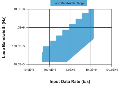
| Option 300 Loop Bandwidth Range Chart Depending on the firmware revision in the mainframe, select one of the following two charts. The instrument automatically calculates the minimum and maximum loop bandwidths to ensure that the module operates within specifications. | |
| Mainframe Firmware Revision A.7.00 and Above. Chart of Selectable Loop Bandwidth Range Versus Data Rate (0.25 ≤ Transition Density ≤ 1) |

|
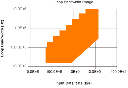
| Mainframe Firmware Revision A.6.01 and Below. Chart of Selectable Loop Bandwidth Range Versus Data Rate (0.5 ≤ Transition Density ≤ 1) |
 |
| Loop Bandwidth Accuracy | |
| Standard | ± 30%, characteristic |
| Option 300 | ± 25% for 0.5 transition density, 155 Mb/s to 11.4 Gb/s data rate, and loop bandwidth
≤
(data rate)/1667. For firmware revisions A.06.01 and below: ± 30% for 0.25 ≤ transition density ≤ 1.0 and all data rates, characteristic. For firmware revisions A.07.00 and above: ± 30% for 0.5 ≤ transition density ≤ 1.0 and all data rates, characteristic. |
| Tracking Range | ±1000 ppm of user-entered data rate |
| Acquisition Range | ±5000 ppm of user-entered data rate |
| Internal Splitter Ratio | 50/50 (characteristic) |
| Minimum Input Level to Acquire Lock | 150 mVpp |
| Input Return Loss | |
| DC to 12 GHz: | 22 dB minimum, characteristic |
| 12 to 20 GHz | 16 dB minimum, characteristic |
| Input Insertion Loss. DC to 20 GHz | 7.8 dB maximum, characteristic |
| Electrical Through-path Digital Amplitude Attenuation | 7.5 dB 20 log (Vamp out/Vamp in) measured with PRBS 23 at 13.5 Gb/s. |
| Front-Panel Recovered Clock Output Amplitude | Maximum: 1 Vpp Minimum: 220 mVpp (300 mVpp, characteristic) |
| Maximum Consecutive Identical Digits (CID) to Acquire Lock | 150 characteristic |
| Front-Panel Recovered Clock Output Divide Ratio (User Selectable). Minimum frequency of divided front-panel clock output is 25 MHz. | |
| 50 Mb/s to 7.1 Gb/s data rates: 7.1 to 13.5 Gb/s data rates: |
N = 1 to 16 N = 2 to 16 |
| Data Input/Output Connectors | 3.5 mm, male |
| Front-Panel Recovered Clock Output Connector | SMA |
| Item | Description |
|---|---|
| Use | Indoor |
| Temperature | |
| Operating Non-operating |
0 °C to +55 °C
–40 °C to +70 °C |
| Altitude | |
| Operating | 4600 m (15,000 ft) |
| Non-Operating | 15,300 m (50,000 ft) |
| Humidity | |
| Operating Non-Operating |
Up to 90% relative humidity at < 35 °C
Up to 90% relative humidity at < 35 °C |
| Net weight | Approximately 1.2 kg (2.6 lb) |
| Shipping weight | Approximately 2.1 kg (4.6 lb) |
| Power requirements | Supplied by mainframe |
| Channel Type | Single-mode and multimode optical; Differential or single-ended electrical (input only, no internal electrical dividers) |
| Maximum Input (characteristic) | |
| Electrical (ac coupled) | 6 Vpp differential
3 Vpp single-ended |
| Optical (input damage level) | 1.5 mW average
15 mW peak |
| Wavelength Range | |
| Single-mode, optical: Multimode, optical: |
1250 nm to 1650 nm 750 nm to 1330 nm |
| If the multimode optical input signal does not have all modes excited in the fiber, the coupling ratio will be reduced and the clock recovery may not acquire lock at minimum specified input levels. It is recommended that an optical mode scrambler be used in such a case. | |
| Data Rates | |
| Standard: Option 200: |
50 Mb/s – 7.1 Gb/s continuous tuning. 50 Mb/s – 13.5 Gb/s continuous tuning. |
| Output Random Jitter (RMS), Internal Recovered Clock Trigger | |
| 50 Mb/s – 4.2 Gb/s: | < 3 mUI 700 fs (0.9 mUI) at 1.25 Gb/s, characteristic) |
| 4.2 Gb/s – 7.2 Gb/s: | < 700 fs (400 fs at 4.25 Gb/s, 500 fs at 2.5 Gb/s, characteristic) |
| 7.2 Gb/s – 11.4 Gb/s: | < 500 fs (300 fs at 10 Gb/s, characteristic) |
| 11.4 Gb/s – 13.5 Gb/s: | < 700 fs |
| Verified with PRBS7 pattern, electrical inputs > 150 mVp-p, and optical inputs > 3 dB above specification for minimum input level to acquire lock. Output jitter verification results of the 83496A can be affected by jitter on the input test signal. | |
| The 83496A will track jitter frequencies inside the loop bandwidth, and the jitter will appear on the recovered clock output. Vertical noise (such as laser RIN) on the input signal will be converted to jitter by the limit amplifier stage on the input of the clock recovery. These effects can be reduced, by lowering the loop bandwidth setting. | |
| Output Random Jitter (RMS), Front Panel Recovered Clock | |
| 50 Mb/s – 4.2 Gb/s: | < 4 mUI 700 fs (0.9 mUI) at 1.25 Gb/s, characteristic) |
| 4.2 Gb/s – 7.2 Gb/s: | < 900 fs (400 fs at 4.25 Gb/s, 500 fs at 2.5 Gb/s, characteristic) |
| 7.2 Gb/s – 11.4 Gb/s: | < 700 fs (300 fs at 10 Gb/s, characteristic) |
| 11.4 Gb/s – 13.5 Gb/s: | < 900 fs |
| Verified with PRBS7 pattern, electrical inputs > 150 mVp-p, and optical inputs > 3 dB above specification for minimum input level to acquire lock. Output jitter verification results of the 83496A can be affected by jitter on the input test signal. | |
| The 83496A will track jitter frequencies inside the loop bandwidth, and the jitter will appear on the recovered clock output. Vertical noise (such as laser RIN) on the input signal will be converted to jitter by the limit amplifier stage on the input of the clock recovery. These effects can be reduced, by lowering the loop bandwidth setting. | |
| Clock Recovery Adjustable Loop Bandwidth Range (user selectable) | |
| Standard: | 270 kHz or 1.5 MHz (characteristic). At rates below 1 Gb/s, loop bandwidth is fixed at 30 kHz when Option 300 is not installed. |
| Option 300: | 15 kHz – 10 MHz continuous tuning (fixed value or constant data rate/N ratio). Without Option 200, loop bandwidth is adjustable from 15 kHz – 6 MHz. Available loop bandwidth settings also depend on the data rate of the input signal. For input data transition density from 0.25 to 1, refer to the Selectable Loop Bandwidth Range Versus Data Rate Chart. |
| Option 300 Loop Bandwidth Range Chart. Depending on the firmware revision in the mainframe, select one of the following two charts. The instrument automatically calculates the minimum and maximum loop bandwidths to ensure that the module operates within specifications. | |
| Mainframe Firmware Revision A.7.00 and Above. Chart of Selectable Loop Bandwidth Range Versus Data Rate (0.25 ≤ Transition Density ≤ 1) |
|
| Mainframe Firmware Revision A.6.01 and Below. Chart of Selectable Loop Bandwidth Range Versus Data Rate (0.5 ≤ Transition Density ≤ 1) |

|
| Loop Bandwidth Accuracy | |
| Standard | ±30%, characteristic |
| Option 300 | ±25% for 0.5 transition density, 155 Mb/s to 11.4 Gb/s data rate, and loop bandwidth ≤ (data rate)/1667. For firmware revisions A.06.01 and below: ± 30% for 0.25 ≤ transition density ≤ 1.0 and all data rates, characteristic For firmware revisions A.07.00 and above: ± 30% for 0.5 ≤ transition density ≤ 1.0 and all data rates, characteristic |
| Tracking Range | ± 1000 ppm of user-entered data rate |
| Acquisition Range | ± 5000 ppm of user-entered data rate |
| Internal Optical Splitter Ratio (tapped/passed through) | |
| Single-mode | 20/80 (characteristic) 50/50 (characteristic, 83496AU-102 modules) |
| Multimode | 30/70 (characteristic) Electrical signals have inputs only (no internal power dividers) |
| Minimum Input Level to Acquire Lock, Voltage or Optical Modulation Amplitude (OMA) | |
| Electrical: | 75 mVpp |
| Single-mode 1310 nm / 1550 nm (OMA): 7.1 Gb/s – 13.5 Gb/s (with Option 200) 1 Gb/s – 7.1 Gb/s 50 Mb/s – 1 Gb/s |
–11 dBm, 50 Mb/s to 11.4 Gb/s. –8 dBm, > 11.4 Gb/s –12 dBm, characteristic –14 dBm, characteristic –15 dBm, characteristic |
| Multimode 1310 nm (OMA): 7.1 Gb/s – 13.5 Gb/s (with Option 200) 1 Gb/s – 7.1 Gb/s 50 Mb/s – 1 Gb/s |
–10 dBm, 50 Mb/s to 11.4 Gb/s. –7 dBm, > 11.4 Gb/s –11 dBm, characteristic –13 dBm, characteristic –14 dBm, characteristic |
| Multimode 850 nm (OMA): 7.1 Gb/s – 13.5 Gb/s (with Option 200) 1 Gb/s – 7.1 Gb/s 50 Mb/s – 1 Gb/s |
–8 dBm, 50 Mb/s to 11.4 Gb/s. –7 dBm, > 11.4 Gb/s –9 dBm, characteristic –11 dBm, characteristic –12 dBm, characteristic |
| To convert from OMA to average power with an extinction ratio of 8.2 dB: Pavg dBm = OMA dBm – 1.68 dB | |
| Input Return Loss | |
| Single-mode, optical Multimode, optical DC to 12 GHz, electrical 12 to 20 GHz, electrical |
20 dB 16 dB 22 dB minimum, characteristic 16 dB minimum, characteristic |
| Input Insertion Loss | |
| Single-mode, optical: Multimode, optical: |
2.5 dB maximum 3 dB maximum |
| Front-Panel Recovered Clock Output Amplitude | Maximum: 1 Vpp Minimum: 220 mVpp (300 mVpp, characteristic) |
| Maximum Consecutive Identical Digits (CID) to Acquire Lock | 150 characteristic |
| Front-Panel Recovered Clock Output Divide Ratio (User Selectable) Minimum frequency of divided front-panel clock output is 25 MHz. | |
| 50 Mb/s to 7.1 Gb/s data rates: 7.1 to 13.5 Gb/s data rates: |
N = 1 to 16 N = 2 to 16 |
| Data Input/Output Connectors | |
| Electrical, input only: Single-mode optical: Multimode optical: |
3.5 mm, male FC/PC 9/125 μm FC/PC 62.5/125 μm Additional optical connector adapter types are also available. |
| Front-Panel Recovered Clock Output Connector | SMA |