Setup Examples
The Option S9x070xB Modulation Distortion application measures the nonlinear behavior of an RF microwave amplifier under a modulated signal.
A modulation file is created, uploaded to a signal generator, then fed into the VNA to test the behavior of the device by measuring band power, ACP, and EVM.
In this topic:
See Also
Example Distortion Setup Procedure
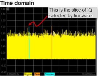
The following example describes how to set up a typical measurement using an N5182B MXG. In this example, a modulation file for a Compact modulation type is created. Compact signals cut a slice of the IQ data from an original waveform. Learn more.
-
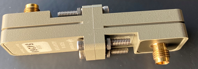
Connect the equipment as shown after this procedure.
-
On the VNA front panel, press Preset.
-
Perform the following steps to set up an external MXG signal generator: See https://www.keisight.com/find/m981xa-install/ when you use M9810A and M9336A in M981xAS.
-
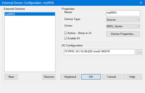
On the VNA front panel, press Setup > External Hardware > External Device....
-
Click on the New button.
-
Click in the Name field and type a name for the source. For example, myMXG.
-
For Device Type, select Source.
-
For the Driver, select MXG_Vector. (When you use VXG or VXT, select VXG or VXT_Vector, respectively)
-
Select Active - Show in UI.
-
Ensure that Enable IO is checked.
-
In the I/O Configuration field, type the VISA address of the MXG.
-
Click on the OK button. The following is an example:
-
On the VNA front panel, press Meas > S-Param > Meas Class....
-
Select Modulation Distortion, then either:
-
The Modulation Distortion Setup dialog will be displayed.
-
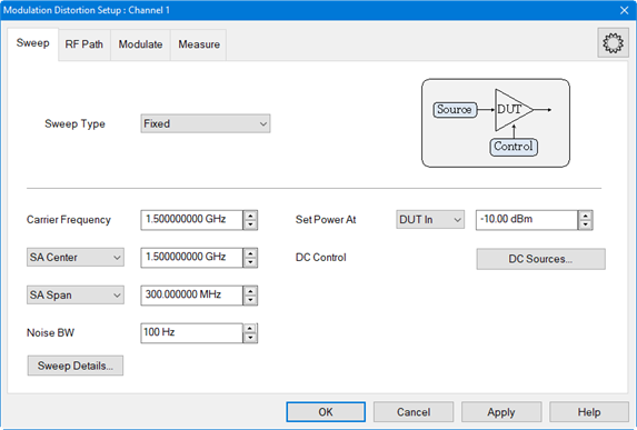
Click on the Sweep tab and define the parameters as shown below:
-
Click on the RF Path tab and define the parameters as shown below:
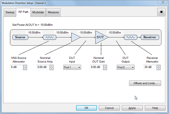
Nominal Src Amp - If there is a loss between the MXG source output and Port 1 of the VNA, then use a negative number. This value is used for power calibration and to set the power level at the output of the DUT..
To access the Offsets and Limits dialog, click on the Offsets and Limits... button.
Nominal DUT Gain - This value is used for power calibration.
-
Click on the Modulate tab.
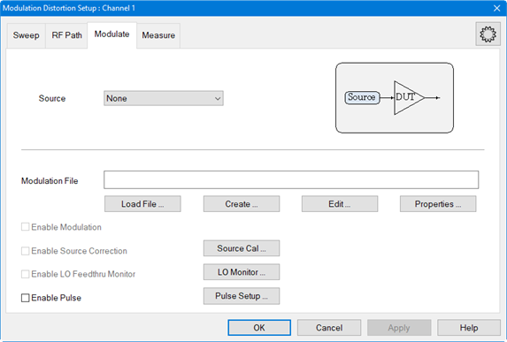
-
Select the MXG source from the Source pull down.
-
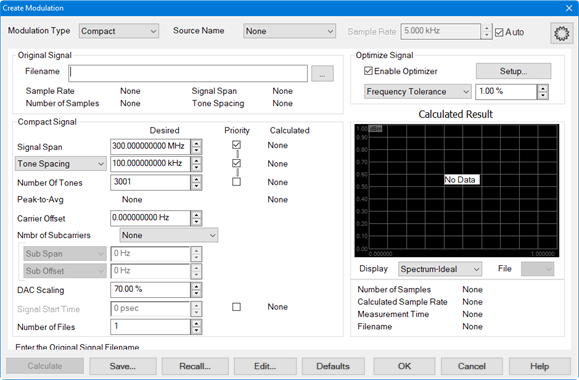
Click on the Create... button to access the Create Modulation dialog.
-
For the Modulation Type, ensure that Compact is selected from the pull down menu. This is the default selection.
-
Click on the "..." button to the right of the Filename field to load the original file from which to create a compact signal.
-
For Signal Span, use the default value.
-
For Tone Spacing and Number of Tones, use the default values.
-
For DAC Scaling, use the default value. For better S/N, increase the scaling value until a DAC overload occurs.
-
For Frequency Tolerance, use default value of 1 %.
-
Click on the Calculate button then verify that the signal is reasonable.
-
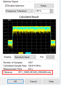
Click the Save... button and save the compact signal file. The filename is displayed below the display window.
-
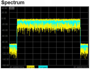
In the Display pull down menu, select Spectrum-Ideal. Signals similar to the following should be displayed:
-
In the Display pull down menu, select Time. Signals similar to the following should be displayed:
-
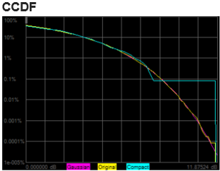
In the Display pull down menu, select CCDF. Signals similar to the following should be displayed:
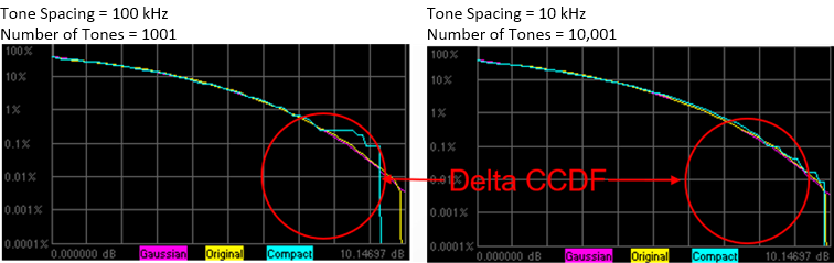
Increasing the number of tones results in the following:
-
In the Create Modulation dialog, click OK.
-
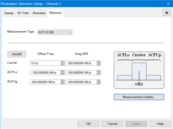
Click on the Measure tab and define the parameters as shown below:
-
Selecting ACP+EVM measures band power, ACP, and EVM for the specified frequency settings in the Measure tab.
-
Click OK.
-
To make a measurement check without calibration, perform the following steps:
-
Make a Thru connection between the Pin and Pout reference planes.
-
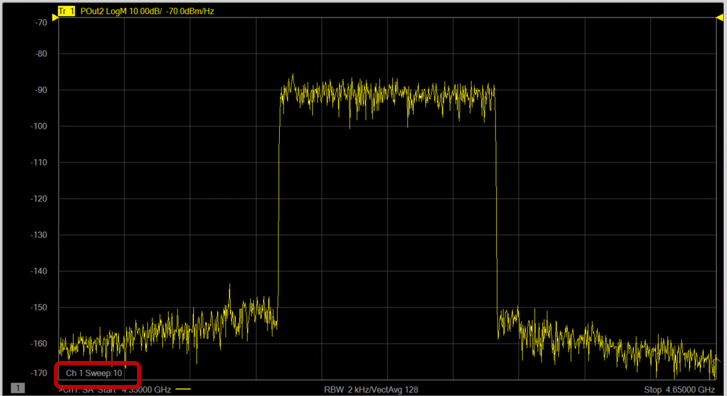
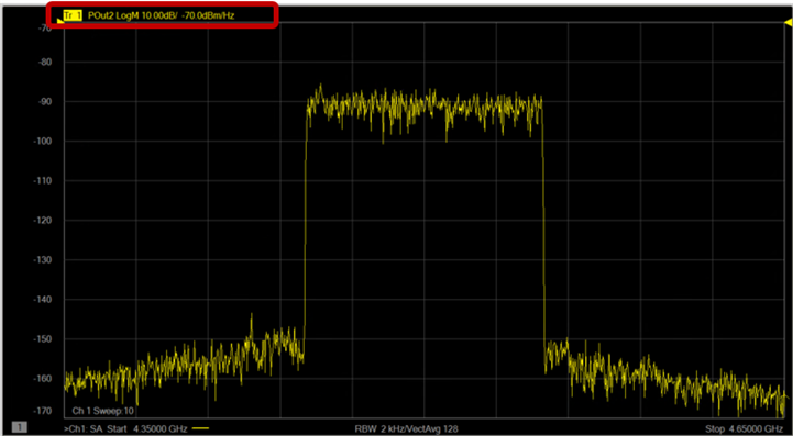
Press Format > Format 1 > Log Mag then select dBm/Hz.
-
Press Scale > Main > Scale then set the scale to 10 dBm Per Division.
-
Press Reference Level then set it to -70 dBm.
-
Press Reference Position then set it to 10 Div.
-
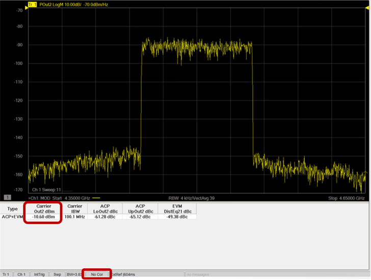
Press Display > Display Setup > Show Table then select Distortion.
-
Note the following:
-
The Modulation Distortion channel makes multiple background sweeps to complete the measurement. During the measurement, the carrier frequency of the compact signal does not change, but the VNA local frequency changes to cover the SA span (300 MHz in this example). The result is stitched together and stored in the Modulation Distortion channel.
-
The Power Spectral Density (PSD) dBm/Hz at the reference plane is displayed.
-
The power level is not calibrated at this point. The result shown is based on the factory calibration of the receiver.
- Refer to S-Parameter Calibration for a procedure on calibrating the VNA receivers.
- After performing an S-parameter calibration, refer to Source Modulation Calibration for a procedure on calibrating source power and flatness.
- After calibration, perform the following steps:
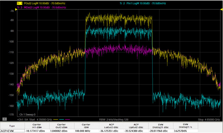
- Press Trace > Trace 1-7 > New Traces....
- In the New Trace dialog, select PIn1 (Power In), POut2 (Power Out) and MDist2 (Modulation Distortion Out).
- Change the format to dBm/Hz.
- Scale as needed.
- If the Distortion Table is not displayed, Press Display > Display Setup > Show Table then select Distortion.
- The following is an example showing input signal and output signal measuring ACPR and EVM.
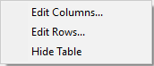
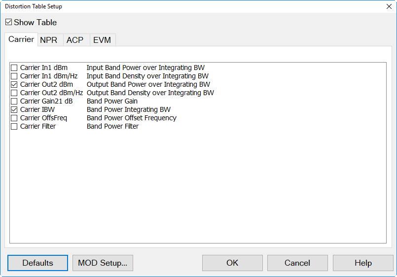
- Add/remove parametric values by right-clicking in the distortion table at the bottom of the measurement area to access the pop up menu then selecting Edit Columns....
- Make desired selections from the Distortion Table Setup dialog.
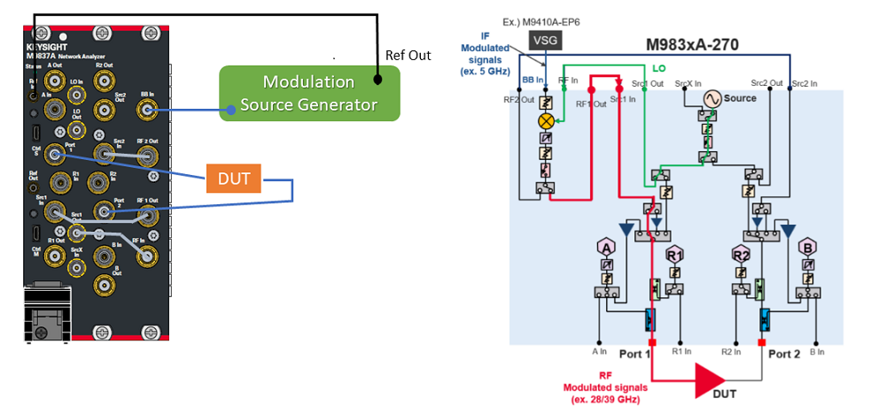
Physical Setup for M983xA-270
The following diagram show the hardware setup for the up-convertor. If the system has a M983xA-270, the up-conversion feature is automatically enabled at MOD/SA multitone measurement. It is integrated to the existing setup flow and UI. There are no dedicated settings on the GUI and SCPI commands.
|
Signal
|
Direction
|
Port
|
From/To
|
|
IF
|
Input
|
BB In
|
Modulated waveform from external VSG
|
|
LO
|
Input
|
Internal
|
Internal CW SRC
|
|
RF
|
Output
|
Test port 1/2 or RF 1/2 Out
|
To DUT
|
The user only needs to set the desired RF output frequency and power. The VNA FW will automatically selects IF and LO settings. Also, it automatically overrides the external VSG settings, to adjust at the VNA RF output plane. There are no interface to manually select the IF and LO frequency.
Path Configurations
To select the source output port, set DUT Input port settings on the MOD RF Path.
For SA multitone measurement, select a transfer switch state in the Path Configuration.
-
GUI: Mixer Switch = "Port1" or "Port2"
-
SCPI: SENS:PATH:CONF:ELEM “Module1MixerTransferSwitch”,”Port1” or “Port2”
To get the signal at RF 1/2 Out port instead of VNA test ports, set Jumper state in the Path Configuration.
Modulation Distortion Convertor Setup
-
The Modulation Distortion Converter feature supports M983xA only. The modules should have Option 190.
-
In the multi-module configuration with M980xA, LO can be supplied from the port of M980xA.
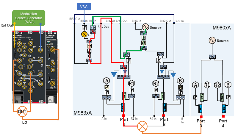
Physical Setup for M980xA
The following diagrams show a typical hardware setup using M980xA VNAs. See PXI VNA Multiport setup also if you configure this with multiple modules.
Physical set setup for M980xA VNA
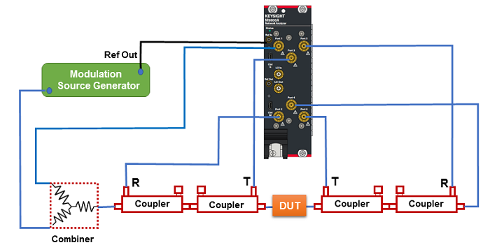
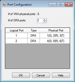
The DRA Port Configuration should be setup as below for this setup.
Physical set setup for the combinations of M980xA VNA and M981xA Receivers
See https://www.keisight.com/find/m981xa-install/ for more detailed setup information.
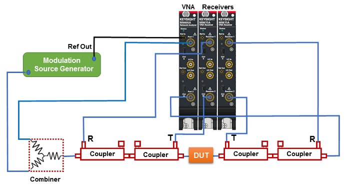
The DRA Port Configuration file should be setup as below for this setup.
<M980X>
<physicalports>6</physicalports>
<dra numports ='2'>
<draports src='1' rcv_r='3' rcv_t='4' />
<draports src='2' rcv_r='5' rcv_t='6' />
</dra>
</M980X>
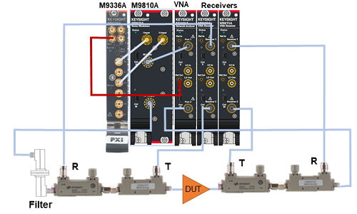
With M981xAS Option 750 (M9810A and M9336A) for Signal Source.
See https://www.keisight.com/find/m981xa-install/. The brief connection is shown in the following figure.
Setup for a wideband amplifier measurement
When measuring wideband amplifier that has a high gain below 20 GHz, it is recommended to add a filter between M9810A RF output and coupler input. This may improve the EVM and/or ACP result.
|
Measurement Frequency Range
|
Recommended Filters
|
|
20 to 26.5 GHz
|
Keysight K281C Coaxial Waveguide Adapter, 2 ea. or equivalent filter (Eravant SCF-15312340-42KFKF-H1, 1ea.)
|
|
26.5 to 40 GHz
|
Keysight R281A Coaxial Waveguide Adapter, 2 ea. or equivalent filter (Eravant SCF-22318340-28KFKF-H1, 1 ea.)
|
|
33 to 44 GHz
|
Keysight Q281A Coaxial Waveguide Adapter, 2 ea. or equivalent filter (Eravant SCF-27324340-222F2F-H1, 1 ea.)
|
Waveguide Filter (High Pass Filter)
Two coaxial waveguide adapters can be a high pass filter.
Example: two R281As (26.5G to 40GHz)