Matching clock-to-data delays for accuracy
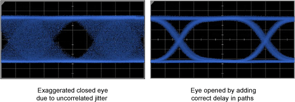
In this topic, you’ll learn how to compensate for the differences in delay between the clock and data paths in your measurement setups. The differences in delay can cause the jitter on clock triggers and data signals to become uncorrelated which can result in closed eyes and reduced measurement accuracy as shown in the following figure. This figure shows an exaggerated worst-case example using a signal with SSC applied. This is a particular problem with low-frequency jitter.
In this topic, you'll learn to identify problems in delay and how to correct the problem. Example test setups are provided for the N1076A/B, N1077A, and N1078A.
Should data and clock paths be matched?
The following table lists conditions in the measurement setup that may require matching of the delay between the clock and data paths. Solutions to mismatched paths include adding cables from a phase matching kit and installing the Precision Timebase Delay Line Assembly on the DCA-X oscilloscope.
| Test Setup Includes | Electrical Input | Optical Input | Phase Matching Kit | PTB Delay Line Assembly |
|---|---|---|---|---|
| N1076A/B, N1077A, or N1078A option JSA with Jitter Optimization turned on. | ♦ | ♦ | ||
| N109x-series DCA-M oscilloscope. | ♦ | ♦ | ||
| Input signal is jitter limited. | ♦ | ♦ | ||
| Input signal has >50% low-frequency jitter | ♦ | ♦ |
Phase Matching Kits
In most situations, differences in delay between the clock and data paths is not a problem and using a good quality 1m cable, instead of an 0.5m cable, between the clock recovery output and your DCA-X oscilloscope is unlikely to impact measurement accuracy. Likewise, using a 1m optical fiber instead of a 3m fiber is unlikely to degrade your optical measurements. Phase matching kits are available for each module.
PTB Delay Line Assembly
The installation of the PTB Delay Line Assembly is described in the N107X-series user's guide, which can be downloaded from keysight.com.
To quickly check for unmatched clock and signal paths
- Change the clock recovery PLL loop bandwidth by a few MHz (for example, from 5 MHz to 10 MHz) while observing Jitter Mode results.
- If Jitter Mode results do not change significantly, matching clock and data paths is not critical.
To check if input signal is jitter limited
- Place the oscilloscope in Eye mode and setup an eye mask test.
- If there is less mask margin due to jitter (horizontal) impairments (more hits on the left/right sides of the mask), your signal is "jitter limited" and would benefit from matching clock and data paths. If more mask hits occur due to amplitude hits (the top/bottom of the mask), matching clock and data paths is unlikely to be critical.
To check the input signal for low-frequency jitter
Significant low-frequency jitter is often the result of using Spread Spectrum Clocking (SSC).
- Place the oscilloscope in Jitter Mode.
- Measure RJ rms with JSA Analysis off (all jitter to module BW).
- Measure RJ rms with JSA Analysis on (low frequency jitter to 26 MHz). Make sure to Jitter Optimization is selected.
- If the RJ rms (on) measurements if >50% of the RJ rms (off) measurement, low-frequency jitter too large. For example, RJ rms measures 600 fs (JSA off) and 450 fs (JSA on). In this case more than 50% of the jitter is coming from "low-frequency" jitter sources and you should match clock-to-data path lengths.