JSA/CRE Concepts
The characteristics of a clock-recovery PLL affect jitter measurements. This is true whether the clock-recovery is part of the DUT, part of a real-time oscilloscope, or part of a sampling oscilloscope such as the N1000A. JSA is a powerful tool that allows you to change the reference signal used for jitter measurements and to change the PLL loop characteristics via Clock Recovery Emulation (CRE).
As with any jitter measurement, the incoming signal is always measured relative to a reference signal (typically a clock). Suppose that we have access to a clean clock and do not need to recover the clock. In the instrument, the phase of the input signal and clock are compared in a sampler. Any jitter on the input signal is detected when its phase is compared to that of the relatively jitter-free clock. Now, let us look at what happens when a clock is not available and we must use clock recovery.
The following figure shows a simplified block diagram of the N1060A module. The input signal is split with one path providing the clock via clock recovery. In the equivalent-time acquisition sampler, the phase of the input signal is compared relative to the phase of the recovered clock. Jitter that is within the clock recovery PLL's loop bandwidth tracks the jitter on the input signal thus decreasing the phase difference observed at the sampler. Jitter that is outside of the loop bandwidth can no longer track the input signal's jitter and jitter on the input signal is transfered to the output of the sampler.
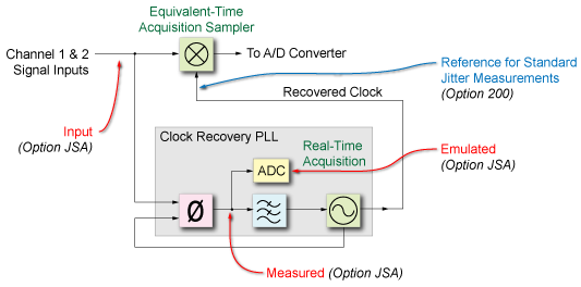
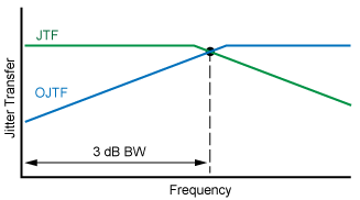
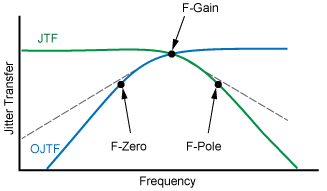
The loop's Jitter Transfer Function (JTF) describes how the clock-recovery PLL affects the jitter on the clock. As jitter decreases on the recovered clock reference signal, the jitter observed at the sampler's output increases. The Observed Jitter Transfer Function (OJTF) describes the transfer of the input signal's jitter to the jitter observed at the sampler's output. The characteristics of the clock-recovery PLL affect the observed jitter spectrum seen at the sampler's output. Hardware clock recovery typically uses a second-order loop which has some amount of peaking near the filter cutoff frequency, which increases the jitter spectrum at this frequency. Many standards call out specific characteristics for a clock-recovery PLL. As you can see, jitter measurements are made relative to the clock at the sampler. This is noted by the blue colored callout in the diagram.
JSA allows you to display the jitter spectrum relative to one of the following three new reference clock signals. These choices are labeled in red in the above simplified block diagram and are selected in the Spectrum Type To Use field of the Jitter Spectrum Analysis Setup dialog:
- Input
- Select to view all of the low- frequency jitter on your signal. Uses a constant clock as the reference. This is the recovered clock with the effects of the clock recovery PLL de-embedded. Configure this reference in the Clock Recovery tab of the 86108A/B Setup dialog. In the dialog's Target LBW field, enter the narrowest loop bandwidth possible while still maintaining lock.
- Measured
- Select to view the low-frequency jitter that is a sub-set of the jitter spectrum that is measured by Jitter Mode. This is the output of the PLL's phase detector is the recovered clock from the hardware clock-recovery circuit as the reference. Configure this reference in the Clock Recovery tab of the N1060A Setup dialog. In the dialog's Target LBW field, enter the specified bandwidth for the applicable standard. In the dialog's Type Two Loop Transition Frequency (Peaking) field, enter the peaking setting recommended by the applicable standard.
- Emulated
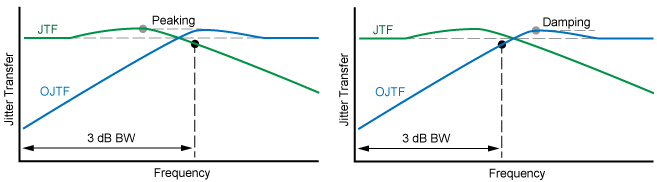
- Select to view low-frequency jitter response to a wide variety of user-specified clock recovery (PLL) configurations. Uses the software Clock Recovery Emulation (CRE) as the reference. To configure the CRE, use the Configure CRE PLL dialog. The following simplified graphs show the Jitter Transfer Function (JTF) and Observed Jitter Transfer Function (OJTF) plots for the 1st, 2nd, and 3rd order loops. The 2nd order loop show peaking and damping.
Use the Jitter Spectrum Analysis Graph to view the observed jitter spectrum based on the input signal referenced to these new types. The JSA graph and scalar results are accomplished by using a real-time acquisition system that resides inside the N1060A's clock-recovery circuit. The Jitter Mode and JSA measurements are made simultaneously, but are performed using independent acquisition systems.
with Zero, Pole, and Gain Frequencies