Combined Loading
The probe load has both resistive and capacitive components. In addition to this, there is inductance in the probe ground lead. The following graphic shows a simplified diagram of the circuit with the probe attached to indicate the principal loading effects.
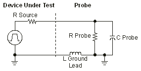
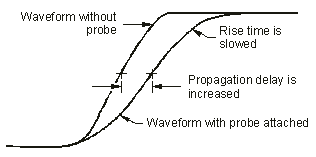
The probe capacitive loading (C probe) to ground forms an RC circuit with the resistance looking into the probe and source (R source). The time constant of this RC circuit slows the rise time of any transitions, decreases the slew rate, and introduces delay in the actual time of transitions. The approximate rise time of a simple RC circuit is 2.2 RC.
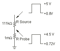
The resistance of the probe to ground forms a divider network with the source resistance of the circuit under test. This reduces the signal amplitude and the DC offset. For example, if the probe's resistance is 9 times the Thevenin output resistance of the circuit under test, the amplitude is reduced by about 10 percent. Therefore, if your waveform has a +5V to +0.8V range, the instrument probe system shows a +4.5V to +0.72V range as shown in the figure below. The following figure shows reduced amplitude and DC offset, the results caused by probe loading.
At high frequencies, the probe reactance dominates the resistance.
The capacitance of the probe tip to ground forms an RC circuit with the output resistance of the circuit under test. The time constant of this RC circuit slows the rise time of any transitions, increases the slew rate, and introduces delay in the actual time of transitions. The approximate 10% to 90% rise time of a simple RC circuit is
where
For example, the actual rise time of a circuit with a resistance of 100 Ω , an instrument probe system resistance of 1 M Ω , and a probe capacitance of 8 pF is
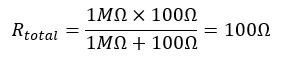
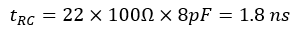
Therefore, for an output resistance of 100 Ω and a probe tip capacitance of 8 pf, the rise time at the node under test cannot be faster than approximately 1.8 ns, although it might be faster without the probe. If the output of the circuit under test is current-limited (as is often the case for CMOS), the slew rate is limited by the relationship dV/dT = I/C. The effects of probe capacitance are displayed in the following figure.
Perhaps you have connected an analyzer to a circuit for troubleshooting only to have the circuit operate correctly after connecting the probes. The capacitive loading of the probes can attenuate a glitch, remove ringing or overshoot, or slow an edge just enough that a setup or hold time violation no longer occurs.
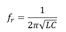
The inductance of the probe ground lead forms an LC circuit with the probe's capacitance and the output capacitance of the circuit under test, including any parasitic capacitance of PC board traces, and so on. The ringing frequency of this circuit is
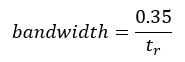
If the rise time of the signal is sufficient to include frequency content sufficient to stimulate this ringing, then it can appear as part of the captured signal. An approximation of the bandwidth of the signal is
To calculate the ringing frequency, assume the probe ground wire has an inductance of approximately 25 nH per inch. Therefore, a probe with a tip capacitance of 8 pF and a 4-inch ground wire has a ringing frequency of approximately 178 MHz (not including the circuit capacitance). In this case, a signal with a rise time of less than 1.9 ns can stimulate ringing.